
Chuck for edge bevel removal and method for centering a wafer prior to edge bevel removal

a technology of edge bevels and chucks, which is applied in the direction of cleaning processes and equipment, cleaning using liquids, chemistry apparatus and processes, etc., can solve the problems of causing scalding, slipping, and affecting the cleaning effect of the chuck, so as to reduce the wear of the suction cup, eliminate curling or rolling of the lip, and prevent particle generation

Active Publication Date: 2017-10-12
LAM RES CORP
View PDF6 Cites 10 Cited by
  • Summary
  • Abstract
  • Description
  • Claims
  • Application Information

AI Technical Summary

Benefits of technology

The patent text describes a method for cleaning a wafer in semiconductor manufacturing. The method includes steps to centering the wafer, using a prerinse liquid to remove any unwanted metal from the edge bevel area of the wafer, and delivering a stream of liquid etchant to remove metal selectively from the edge bevel area. The method also involves using elastomeric suction cups to hold the wafer in place during centering, which can cause particle generation. By flowing nitrogen gas out of the suction cups, the method reduces wear and prevents particle generation, and also ensures a smooth movement of the wafer over the support pins.

Problems solved by technology

This causes the wafer to “stick and slip” which creates particles.

Method used


Image

  • Chuck for edge bevel removal and method for centering a wafer prior to edge bevel removal
  • Chuck for edge bevel removal and method for centering a wafer prior to edge bevel removal
  • Chuck for edge bevel removal and method for centering a wafer prior to edge bevel removal

Examples


Embodiment Construction

[0020]In the following detailed description, numerous specific embodiments are set forth in order to provide a thorough understanding of embodiments described herein. However, as will be apparent to those skilled in the art, the claimed invention may be practiced without these specific details or by using alternate elements or processes. In other instances well-known processes, procedures and components have not been described in detail so as not to unnecessarily obscure aspects of the claimed invention.

[0021]A “semiconductor wafer” as referred to herein is a semiconductor substrate at any of the various states of manufacture in the production of integrated circuits. One standard semiconductor wafer described in this invention is 300 mm in diameter, 0.75 mm in thickness, with an approximate radius of curvature of about 0.15 millimeters (see SEMI Specification M1.15-0997). Of course, semiconductor wafers of other dimensions, such as a standard 200 mm diameter silicon wafers, can also...


PUM


Abstract

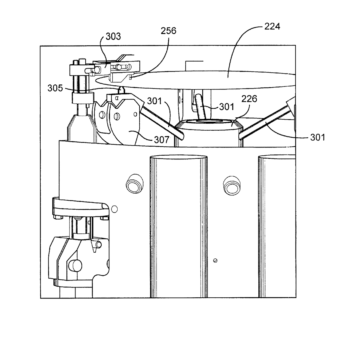
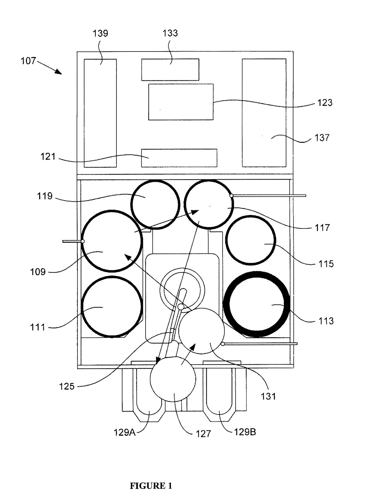
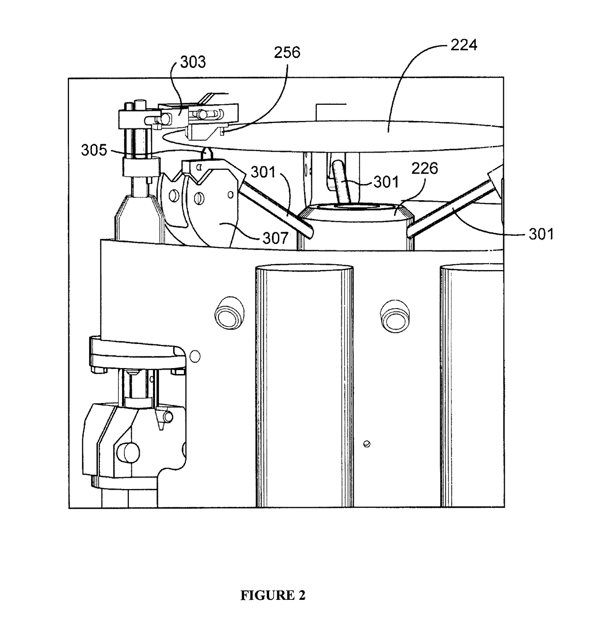
A chuck useful for supporting a wafer during an edge bevel removal (EBR) process comprises a rotatable center hub having a plurality of support arms extending outwardly from the rotatable center hub, support pins on ends of the support arms, gas passages extending through upper surfaces of the support pins, and gas conduits in the support arms, the gas conduits configured to supply gas to the gas passages or apply a vacuum to the gas passages. The support arms can include alignment cams which are rotatable from an outer non-alignment position away from a periphery of the wafer to an inner alignment position at which the wafer is centered. To supply gas or apply a vacuum force to the gas outlets in the support pins, the rotatable center hub can have a gas inlet and a plurality of gas delivery ports in fluid communication with the gas delivery conduits in the support arms. Gas can be supplied to the gas outlets by a source of pressurized gas connected to the gas inlet and suction can be applied to the gas outlets by a vacuum source connected to the gas inlet. During centering, the wafer is floated on a gas cushion which reduces wear of the support pins.

Description

FIELD OF THE INVENTION[0001]This invention relates to chuck technology for supporting semiconductor wafers. More particularly, it pertains to a method of centering a wafer prior to an edge bevel removal (EBR) process wherein liquid etchants remove unwanted metal for the outer edge of a wafer.BACKGROUND[0002]In a typical copper Damascene process, the formation of the desired conductive routes generally begins with a thin physical vapor deposition (PVD) of the metal, followed by a thicker electrofill layer (which is formed by electroplating). The PVD process is typically sputtering. In order to maximize the size of the wafer's useable area (sometimes referred to herein as the “active surface region”) and, thereby, maximize the number of integrated circuits produced per wafer), the electrofilled metal must be deposited to very near the edge of the semiconductor wafer. Thus, it is necessary to allow physical vapor deposition of the metal over the entire front side of the wafer. As a byp...

Claims


Application Information

Patent Timeline
Patent Type & Authority Applications(United States)
IPC IPC(8): H01L21/683H01L21/67B08B3/08H01L21/02
CPCH01L21/6838B08B3/08H01L21/6704H01L21/02041H01L21/67023H01L21/67075H01L21/6875H01L21/6708H01L21/68728H01L21/682H01L21/68785H01L21/6835
Inventor LABRIE, AARON LOUISBRAENDLE, ROBERT LYNDENSWEENEY, CIAN OWEN
Owner LAM RES CORP
Learn More