Etching agent for semiconductor substrate

a technology of etching agent and semiconductor substrate, which is applied in the direction of semiconductor devices, electrical devices, chemistry apparatus and processes, etc., can solve problems such as quality fluctuations, and achieve the effects of reducing surface defects, excellent productivity, and shortening the amount of tim

Inactive Publication Date: 2017-10-26
SETTSU OIL MILL
View PDF3 Cites 0 Cited by
  • Summary
  • Abstract
  • Description
  • Claims
  • Application Information

AI Technical Summary

Benefits of technology

[0020]According to the present invention, some effects are exhibited that the texture formation is made possible to a semiconductor substrate for solar cells at relatively lower temperatures with a shorter amount of time, thereby having excellent productivity. The present invention is effective in both the monocrystalline silicon and the polycrystalline silicon. In addition, pyramidal ruggedness of an average of 5 μm or less is stably formed, so that surface

Problems solved by technology

However, since isopropyl alcohol (IPA) is used, this method has some disadvantages in the aspect of fluctuations of qualit

Method used


Image

  • Etching agent for semiconductor substrate
  • Etching agent for semiconductor substrate
  • Etching agent for semiconductor substrate

Examples


examples

[0112]The present invention will be described more specifically hereinbelow by means of Examples, and these Examples are intended to be illustratively given.

example 44

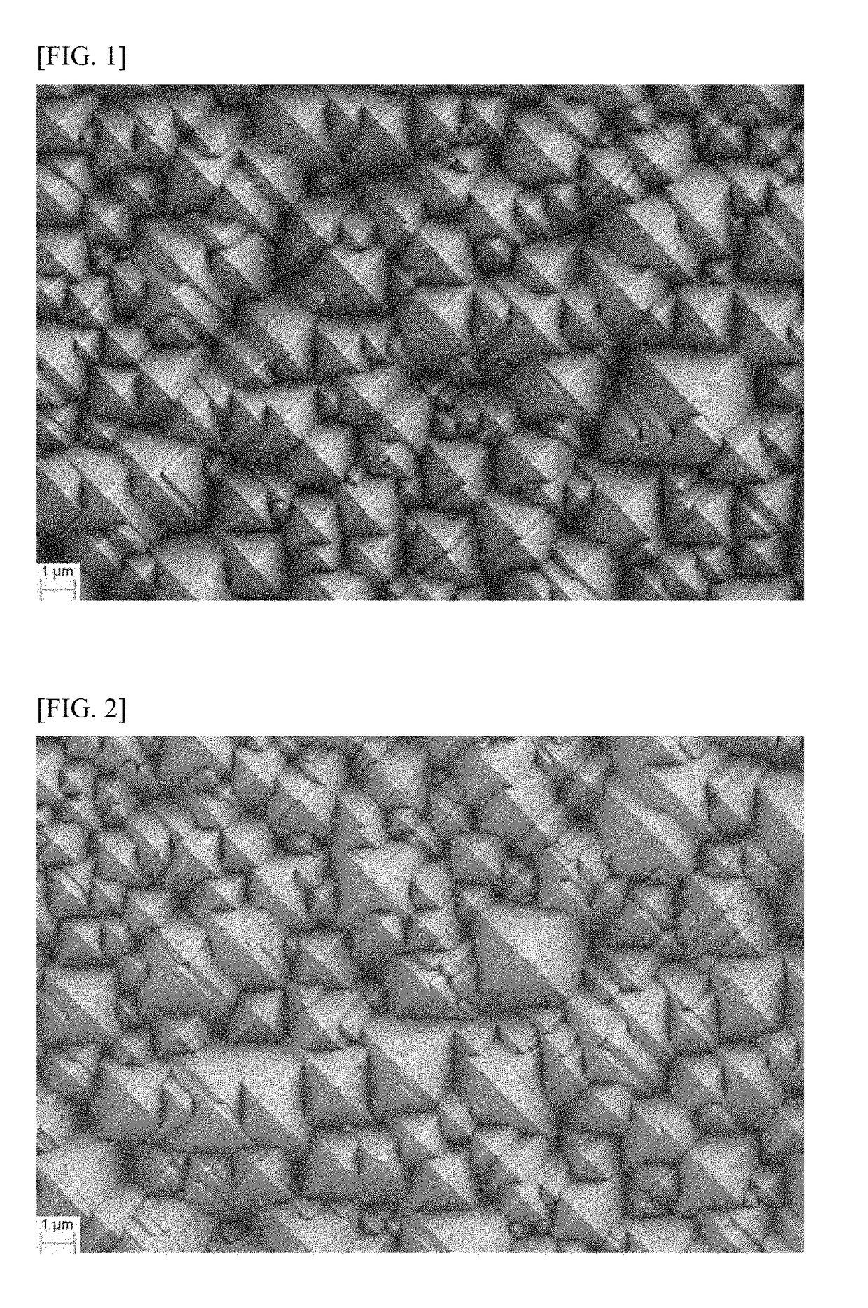
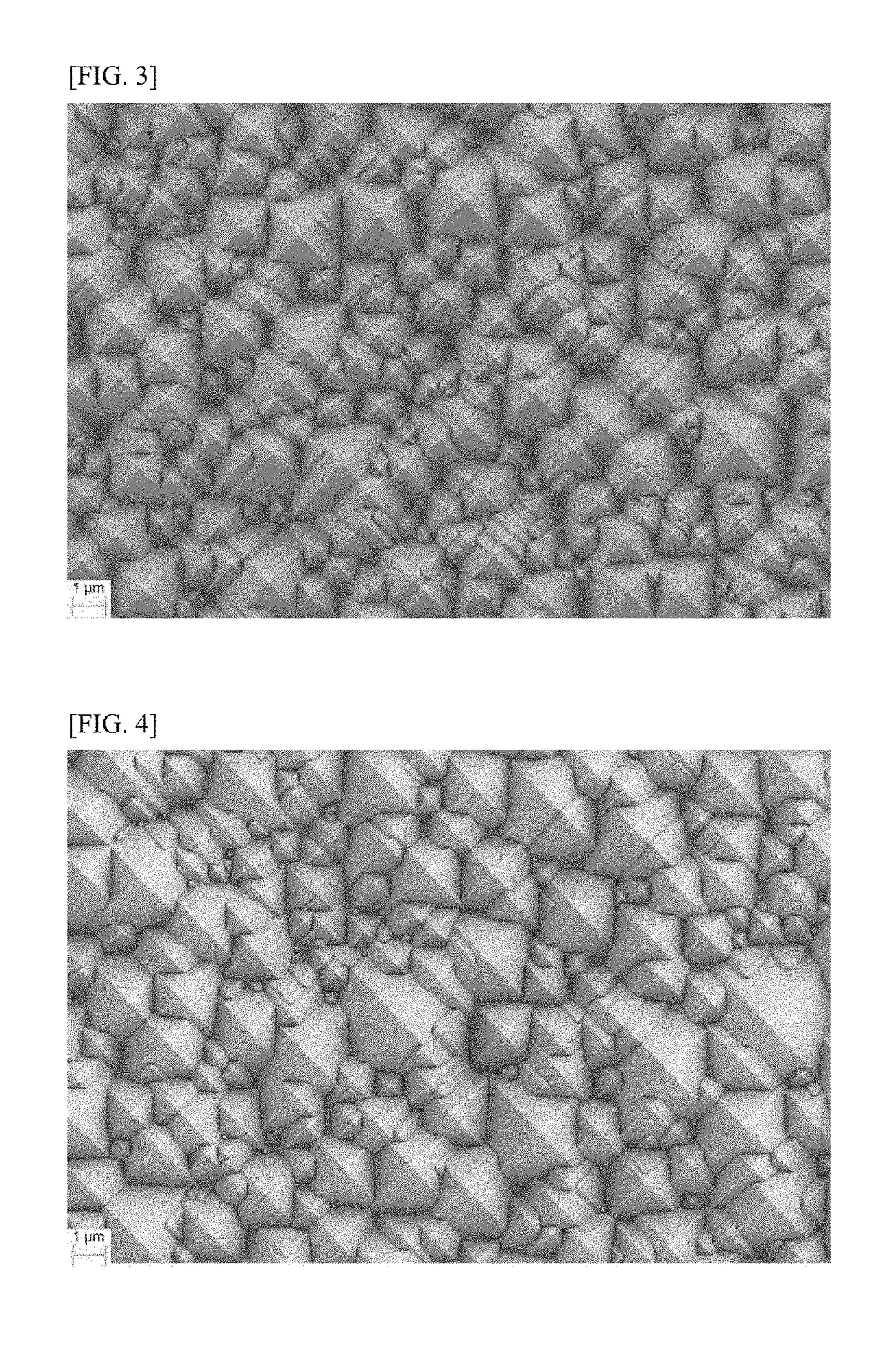
[0116]With regard to staminal property (continuous use) of the etching agent, a plural number of the above silicon substrates were set on a cassette for substrate support (at most 30 disks / cassette) to the original etching agent having a liquid volume of 30 L, and plural batches of treatment were carried out in which one batch is defined as the set cassette. During that treatment, since the consumption of the alkali was tremendously large, the consumed KOH was determined by an automatic titration apparatus, and KOH of a corresponding amount was resupplied every batch. The composition of the original etching agent and the evaluation results is listed in Table 2. Here, the procedures for the specific etching treatment were as described in [Etching Treatment] set forth below. The pH of the etching agent in Example 44 at 25° C. was 13.5.

TABLE 2-1Number ofPolyhydroxy-Batches ofKOHstyreneLignin-ChelatingContinuous% byComponentsulfonateAgentUseweightKindsppmKindsppmppmEx.13a2000A20—44103a2...


PUM


Abstract

The present invention relates to an alkaline etching agent for treating a surface of a semiconductor substrate for solar cells, containing at least one hydroxystyrene polymer represented by the general formula (1) and an alkaline agent. According to the present invention, some effects are exhibited that the texture formation is made possible to a semiconductor substrate for solar cells at relatively lower temperatures with a shorter amount of time, thereby having excellent productivity.

Description

TECHNICAL FIELD[0001]The present invention relates to an etching agent for semiconductor substrates, especially an etching agent for semiconductor substrates for solar cells. Further, the present invention relates to an etching ability restoring agent, a method for producing a semiconductor substrate for solar cells, and a semiconductor substrate for solar cells.BACKGROUND OF THE INVENTION[0002]In order to increase power generation efficiencies of solar cells, conventionally, a method in which ruggedness is formed on the surface of a semiconductor substrate for solar cells, and incident light from the substrate surface is efficiently incorporated into an internal of the substrate has been employed. As a method of uniformly forming fine ruggedness on a substrate surface, a method including subjecting a (100) plane of a monocrystalline silicon substrate with an anisotropoic etching treatment using a mixed aqueous solution of sodium hydroxide and isopropyl alcohol, to form ruggedness o...

Claims


Application Information

Patent Timeline
IPC IPC(8): C09K13/02H01L31/0368H01L31/0236H01L31/028H01L31/18H01L31/068
CPCC09K13/02H01L31/02363H01L31/068H01L31/028H01L31/03682H01L31/1804C09K13/00Y02E10/546Y02E10/547Y02E10/50
Inventor AKAGI, SEIMEIKAMADA, YOSHITERUOHYAGI, NOBORUSAIDA, TOSHINORIMORIWAKI, KAZUHIROYAMAMOTO, YUZO
Owner SETTSU OIL MILL
Why Eureka
Try Eureka