

A full voltage segmented linear constant-current LED drive circuit in auto switchover mode
a technology of led drive circuit and constant-current led drive, which is applied in the field of lighting, can solve the problem of relatively high cost of led drive circuit, and achieve the effect of reducing harmonic distortion
- Summary
- Abstract
- Description
- Claims
- Application Information
AI Technical Summary
Benefits of technology
Problems solved by technology
Method used
Image

Examples
embodiment 1
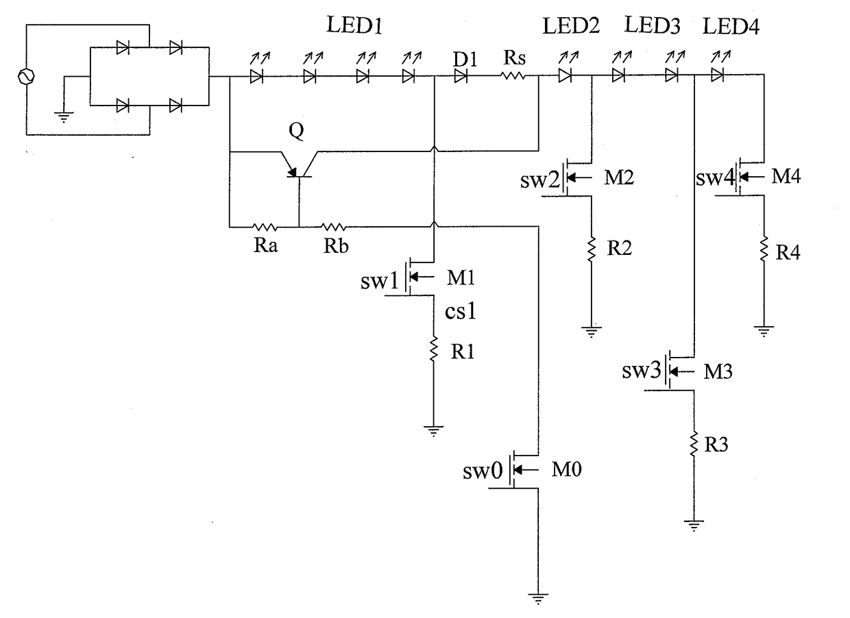
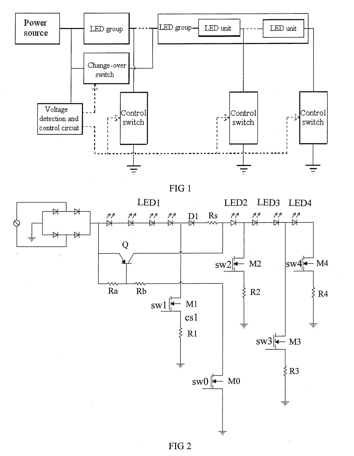
[0047]Referring to FIG. 2, it is applicable to set V0=200V in case of 120V and 277V AC voltages. The output of AC power subjecting to rectification is as shown on the left side of the figure; all LEDs are divided into two groups; wherein the 1st group is LED1 (specifically comprising 4 LEDs), and others fall into the 2nd group; the 2nd group is divided into three units, namely unit LED2 (specifically comprising 1 LED), unit LED3 (specifically comprising 2 LEDs) and unit LED 4 (specifically comprising 1 LED); all LEDs are in series connection in proper sequence; an anti-reflux triode D1 and resistor Rs are in series connection between the 1st and 2nd groups.
[0048]The change-over switch comprises a triode Q and MOS M0; wherein, the collector and emitter of triode Q are connected to the positive terminal of the 2nd group of LED and output terminal of a power source; whereas the base is connected to the output terminal of the power source via the 1st voltage division resistor Ra;
[0049]T...
embodiment 2
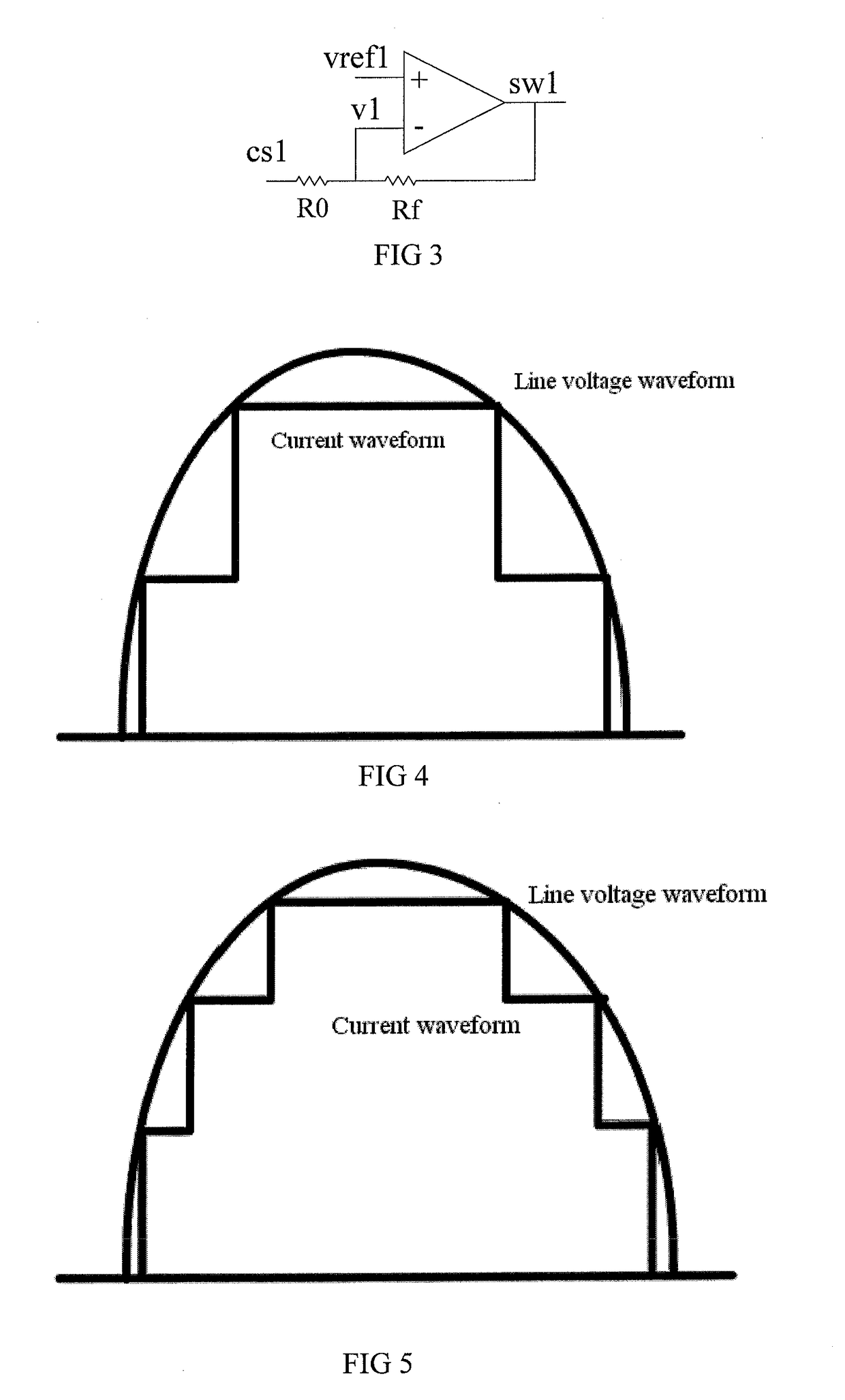
[0069]In embodiment 1, the logic of MOS M0 and M1 can be deemed as being basically identical in case of 120V and 277V; the only difference is that MOS M1 is provided with current limiting function that is unavailable for MOS M0; such difference will not result in logic variation to other control switches.
[0070]Referring to FIG. 6, MOS M0 and M1 in the embodiment is replaced by only one MOS; such MOS can be MOS M1; to guard against reflux, diode D6 is provided between negative terminal of the 1st group of LEDs and MOS M1. This can simplify peripheral circuit, and reduce cost for peripheral circuits.
embodiment 3
[0071]Referring to FIG. 6, grounding mode for the control switch of each LED unit in this embodiment is different from that in Embodiment 2; in other words, the current limiting value is different.
[0072]As shown in the figure, the negative terminal of resistor R2 is connected between MOS M3 and sampling resistor R3; whereas the negative terminal of sampling resistor R3 is connected between MOS M4 and sampling resistor R4.
[0073]As compared with linear voltage detection, such structure has the following advantage: As several MOSs are available for auto switchover regardless of output voltage from the power source, it is applicable to define the number of LEDs more freely.
PUM
 Abstract
Description
Claims
Application Information