Piezoelectric thin film resonator, filter, and multiplexer
- Summary
- Abstract
- Description
- Claims
- Application Information
AI Technical Summary
Benefits of technology
Problems solved by technology
Method used
Image

Examples
first embodiment
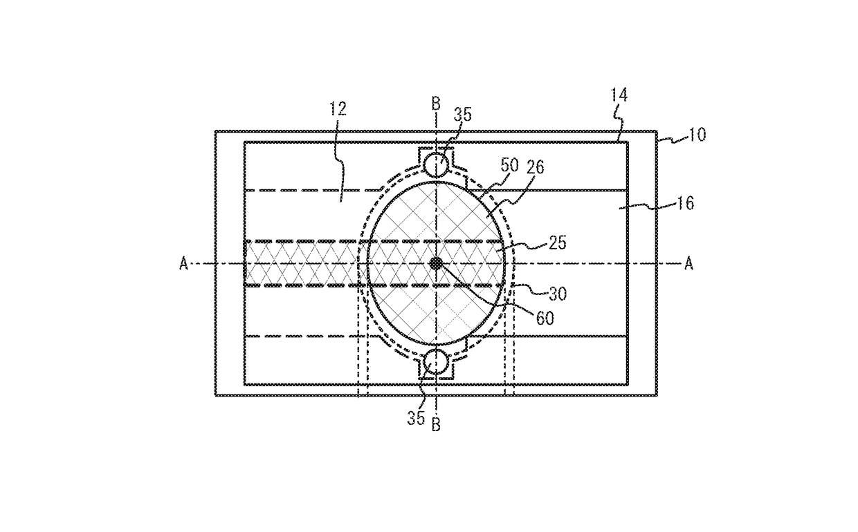
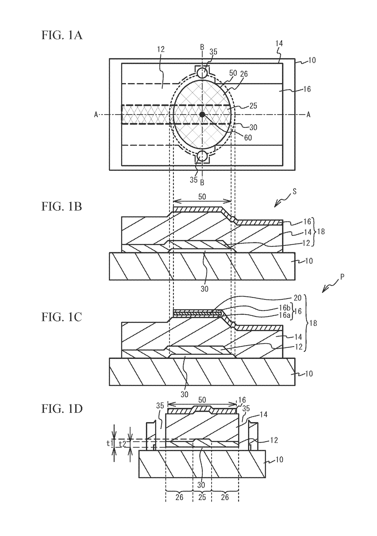
[0031]FIG. 1A is a plan view of a piezoelectric thin film resonator in accordance with a first embodiment, FIG. 1B and FIG. 1C are cross-sectional views taken along line A-A in FIG. 1A, and FIG. 1D is a cross-sectional view taken along line B-B in FIG. 1A. FIG. 1B illustrates, for example, a series resonator of a ladder-type filter, and FIG. 1C illustrates, for example, a parallel resonator of a ladder-type filter.
[0032]With reference to FIG. 1A, FIG. 1B, and FIG. 1D, the structure of a series resonator S will be described. A lower electrode 12 is located on a substrate 10 that is a silicon (Si) substrate. An air gap 30 having a dome-shaped bulge is formed between the flat principal surface of the substrate 10 and the lower electrode 12. The dome-shaped bulge is a bulge having a shape in which the height of the air gap 30 is low in the periphery of the air gap 30, and increases at distances closer to the center of the air gap 30, for example. FIG. 1B through FIG. 1D illustrate a dom...
second embodiment
[0079]A second embodiment changes the structures of the thick film part 25 and the thin film part 26. FIG. 10A is a cross-sectional view of a piezoelectric thin film resonator in accordance with the second embodiment, and FIG. 10B through FIG. 10D are cross-sectional views illustrating a method of fabricating the piezoelectric thin film resonator in accordance with the second embodiment. As illustrated in FIG. 10A, a metal film 27a with a uniform film thickness is located in the thick film part 25 and the thin film part 26. In the thick film part 25, a metal film 27b is located on the metal film 27a. In the thin film part 26, the metal film 27b is not formed. The lower electrode 12 includes the metal films 27a and 27b. Other structures are the same as those of the first embodiment, and the description thereof is thus omitted.
[0080]As illustrated in FIG. 10B, the metal film 27a is formed on the sacrifice layer 38 and the substrate 10 after the step of FIG. 2A in the first embodiment....
third embodiment
[0089]A third embodiment provides an insertion film. FIG. 13A is a plan view of a piezoelectric thin film resonator in accordance with the third embodiment, and FIG. 13B is a cross-sectional view taken along line A-A in FIG. 13A. As illustrated in FIG. 13A and FIG. 13B, the piezoelectric film 14 includes a lower piezoelectric film 14a and an upper piezoelectric film 14b. An insertion film 29 is located between the lower piezoelectric film 14a and the upper piezoelectric film 14b. The insertion film 29 is located in an outer peripheral region 52 in the resonance region 50, and is not located in a central region 54. The outer peripheral region 52 is a region within the resonance region 50, includes the outer periphery of the resonance region 50, and is located along the outer periphery. The outer peripheral region 52 has, for example, a strip shape or a ring shape. The central region 54 is a region within the resonance region 50, and includes the center of the resonance region 50. The...
PUM
 Abstract
Description
Claims
Application Information
 - R&D Engineer
- R&D Manager
- IP Professional
- Industry Leading Data Capabilities
- Powerful AI technology
- Patent DNA Extraction
Browse by: Latest US Patents, China's latest patents, Technical Efficacy Thesaurus, Application Domain, Technology Topic.
© 2024 PatSnap. All rights reserved.Legal|Privacy policy|Modern Slavery Act Transparency Statement|Sitemap