Multilayer ceramic capacitor and manufacturing method of multilayer ceramic capacitor
a manufacturing method and ceramic capacitor technology, applied in the direction of fixed capacitors, stacked capacitors, fixed capacitor details, etc., can solve the problems of inferior plating caused by surface elution of glass, chip seal properties may be affected,
- Summary
- Abstract
- Description
- Claims
- Application Information
AI Technical Summary
Benefits of technology
Problems solved by technology
Method used
Image
Examples
embodiment
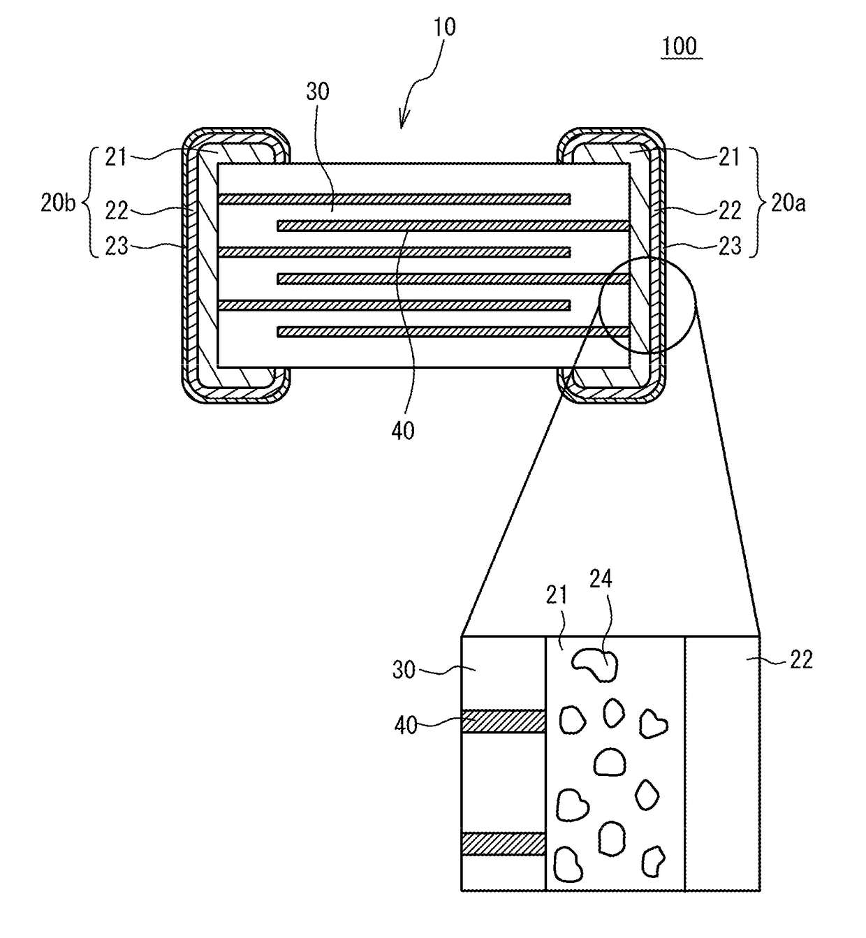
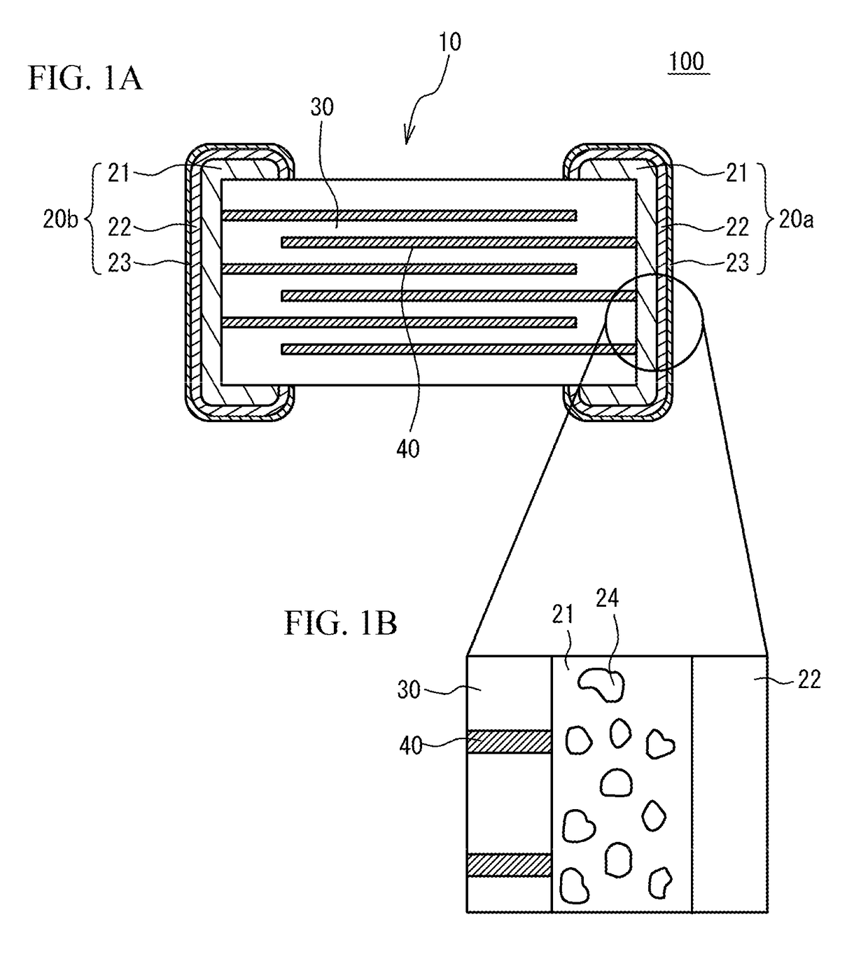
[0014]FIG. 1A and FIG. 1B illustrate a multilayer ceramic capacitor 100 in accordance with an embodiment. The multilayer ceramic capacitor 100 illustrated in FIG. 1A and FIG. 1B is one example. Therefore, the multilayer ceramic capacitor 100 may be applied to shapes other than that of FIG. 1A and FIG. 1B. The multilayer ceramic capacitor 100 may be used for an array.
[0015]As illustrated in FIG. 1A, the multilayer ceramic capacitor 100 includes a ceramic multilayer structure 10 having a rectangular parallelepiped shape, and at least a pair of external electrodes 20a and 20b. The ceramic multilayer structure 10 has a structure designed to have ceramic dielectric layers 30 and internal electrode layers 40 alternately stacked. End edges of the internal electrode layers 40 are alternately exposed to a first end face of the ceramic multilayer structure 10 and a second end face of the ceramic multilayer structure 10 that is different from the first end face. In the embodiment, the first fa...
examples
[0032]The multilayer ceramic capacitors were manufactured in accordance with the embodiment. And characteristic of the multilayer ceramic capacitors was measured.
examples 1 to 11
[0033]The multilayer ceramic capacitors 100 were manufactured in accordance with the embodiment.
[0034]CaZrO3 was used as the ceramic material that is the main component of the ceramic dielectric layer 30. A molar ratio of Zr to Ca (Ca / Zr) was 1.05. BN (3.5 mol %), SiO2 (3.5 mol %), Li2CO3 (1.75 mol %) and MnCO3 (3.5 mol %) were added to the ceramic dielectric layer 30 as the additive material. Cu was used as the main component of the internal electrode layer 40. Cu was used as the main component of the base conductive layer 21 of the external electrodes 20a and 20b. BaO—ZrO based glass component was added to the base conductive layer 21 by 3 to 6 weight part as the sintering agent. Cu was used as the first plated film 22. In any of the examples 1 to 11, the thickness of the first plated film 22 is half of the thickness of the base conductive layer 21 or more. Sn was used as the second plated film 23. In any of the examples 1 to 11, the thickness of the second plated film 23 was 2.5 ...
PUM
| Property | Measurement | Unit |
|---|---|---|
| grain size | aaaaa | aaaaa |
| longitudinal length | aaaaa | aaaaa |
| thickness | aaaaa | aaaaa |
Abstract
Description
Claims
Application Information


