Semiconductor device and multi-chip module

a technology of semiconductor devices and modules, applied in the field of semiconductor devices and multi-chip modules, can solve the problems of not always easy to clarify the correlation between a function defect and a wiring defect, and the multi-chip module becomes a defective produ

Active Publication Date: 2017-12-07
HITACHI LTD
View PDF3 Cites 10 Cited by
  • Summary
  • Abstract
  • Description
  • Claims
  • Application Information

AI Technical Summary

Benefits of technology

[0016]When the present invention is applied, a device that monitors the connection states of the power supply pine, the ground pin, and the signal pin is provided. Such a device can be applied to a wide range of semiconductor products such as information devices, infrastructure control devices, and in-vehicle devices.

Problems solved by technology

If a wiring has a defect, even if each chip has no defect, a multi-chip module becomes a defective product.
However, it is not always easy to clarify a correlation between a function defect and a wiring defect.

Method used


Image

  • Semiconductor device and multi-chip module
  • Semiconductor device and multi-chip module
  • Semiconductor device and multi-chip module

Examples


first embodiment

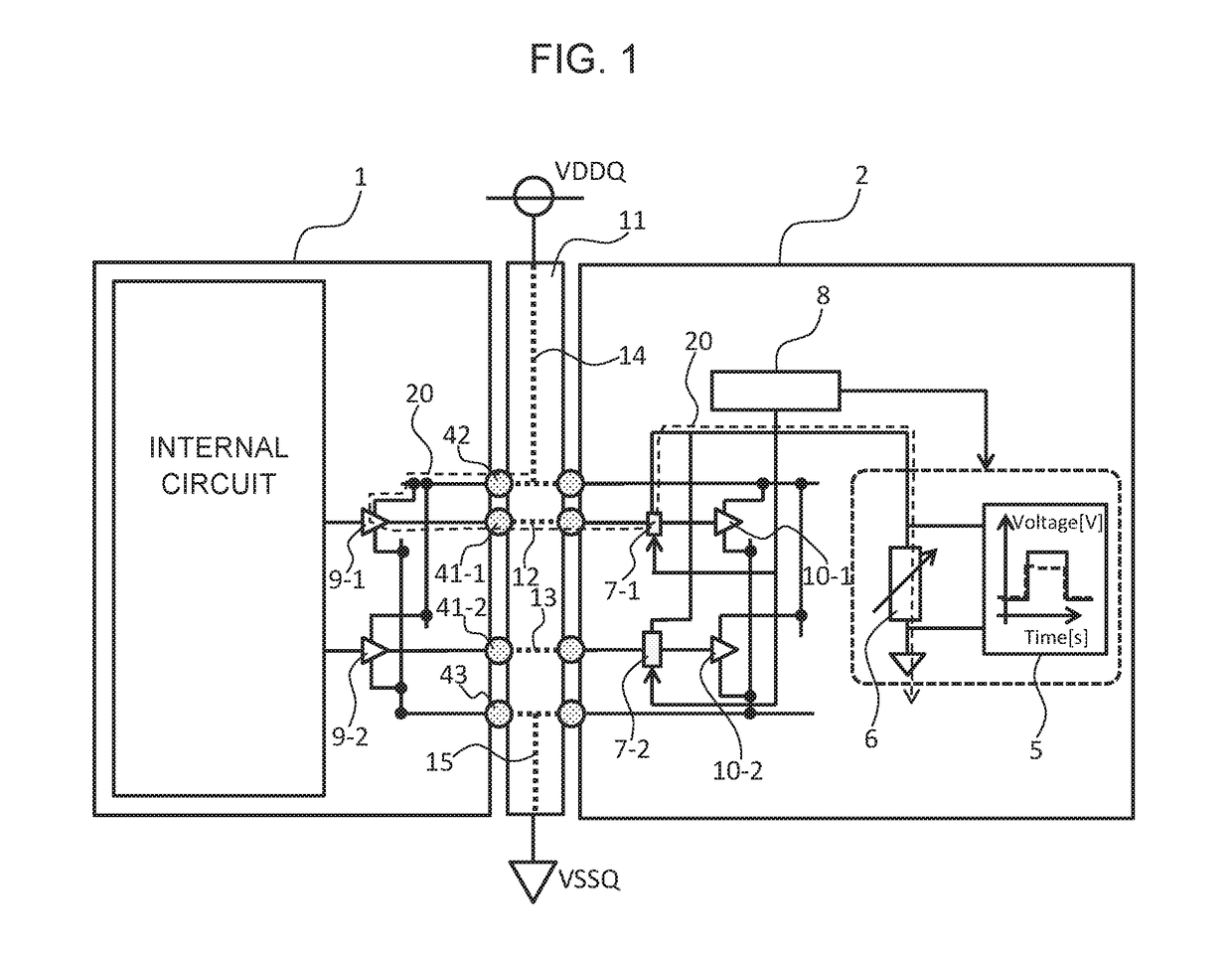
[0032]FIG. 1 illustrates a basic circuit configuration according to a first embodiment as an embodiment of the present invention. As a specific example of this embodiment, as illustrated in FIG. 8, for example, in a system in package (SiP) including a DRAM DIE 1 mounted on a Si interposer 11 and an ASIC DIE 2 that performs various controls, a circuit that monitors all signal connections via the Si interposer 11 and a connection state between a power voltage VDDQ supplied from the Si interposer 11 and a ground potential VSSQ is provided.

[0033]FIG. 1 illustrates a configuration in which a first circuit block 1 and a second circuit block 2 are electrically connected via a wiring block 11 in a broader sense. Power supply to the first circuit block 1 and the second circuit block 2 is performed via the wiring block 11. In this configuration, an example of one-way communication case in which the first circuit block 1 includes output circuits 9-1 and 9-2, and the second circuit block 2 incl...

second embodiment

[0073]FIG. 8 illustrates a second embodiment of the present invention and is a cross-sectional view when the present invention is applied to a system in package (SiP).

[0074]In this case, a semiconductor circuit block can be considered to be a plurality of LSIs mounted on an interposer.

[0075]In this configuration, connection paths 12, 13, 14, and 15 between the first circuit block 1 and the second circuit block 2 of FIG. 1 include a microbump connecting each LSI with the interposer and a wiring in the interposer. However, the inspection circuit of the present embodiment is mainly suitable for monitoring the connection state of the microbump portion connecting LSI with interposer.

[0076]Although FIG. 8 illustrates an example of one-way transmission using two LSIs, the number of LSIs and the signal transmission direction may be arbitrary and, for example, bidirectional.

third embodiment

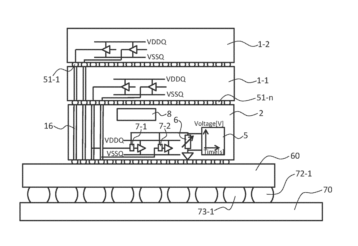
[0077]FIG. 9 illustrates an example in which the present invention is applied to connection between LSIs configured such a plurality of DRAM DIEs 1-1 and 1-2 (up to about 8 DRAM DIEs) are three-dimensionally stacked on a ASIC DIE 2 as a third embodiment of the present invention. In this embodiment, it is also possible to monitor a connection state of a through silicon vias TSV 16 for connecting the upper and lower LSIs.


PUM


Abstract

Provided is a semiconductor inspection circuit which is capable of inspecting connection states of power supply, ground, and signal bumps in a semiconductor package or a printed circuit board equipped with a semiconductor LSI mounted in a product operation state. As a means to solve the problem, a circuit capable of switching a path is provided at an input portion of a driver / receiver, a mechanism capable of transferring an output of a path switching circuit near a receiver circuit to a voltage waveform circuit with an internal variable terminal is provided, and a breakage state of a bump can be observed in the product operation state by observing a DC level at a terminal having a certain DC resistance when a signal bump connection state is observed and receiving a step wave and observing a response waveform thereof when an IO power supply bump connection state is observed.

Description

TECHNICAL FIELD[0001]The present disclosure relates to a technique for monitoring the connection state of a wiring path and identifying an abnormal portion in a semiconductor LSI, a semiconductor LSI package, and a printed circuit board which are used for an information device, an infrastructure control device, an automobile, or the like.BACKGROUND ART[0002]A multi-chip module in which a plurality of semiconductor integrated circuit chips are incorporated into one package is provided with wirings for connecting the chips in the package. If a wiring has a defect, even if each chip has no defect, a multi-chip module becomes a defective product.[0003]Such a wiring defect can be detected by a function test which is performed on the entire package. However, it is not always easy to clarify a correlation between a function defect and a wiring defect.[0004]As background technology of the present technical field, there is JP 2008-122338 A (Patent Document 1). JP 2008-122338 A discloses a te...

Claims


Application Information

Patent Timeline
Patent Type & Authority Applications(United States)
IPC IPC(8): G01R31/04G01R31/28H01L23/00H01L25/065H01L23/498
CPCG01R31/041H01L25/0655H01L23/49838H01L24/16H01L2225/06517G01R31/2851H01L2224/1623H01L2225/06513H01L2225/06541H01L25/0657G01R31/2853H01L2224/13025H01L2224/16146H01L2224/16227H01L2224/17181H01L2924/15192H01L2924/15311G01R31/54G01R31/52G01R31/67
Inventor UEMATSU, YUTAKAOSAKA, HIDEKITOBA, TADANOBUSHIMBO, KENICHI
Owner HITACHI LTD
Why Eureka
Try Eureka