Supercharge Your Innovation With Domain-Expert AI Agents!

Electroconductive film laminate comprising transparent pressure-sensitive adhesive layer

a technology of adhesive layer and conductive film, which is applied in the direction of film/foil adhesive, conductive layer on insulating support, synthetic resin layered products, etc., can solve the problems of poor pattern invisibility, deterioration of properties, and the cost of composition itself, so as to suppress reflection, suppress interface reflection, and high refractive index

Inactive Publication Date: 2017-12-21
NITTO DENKO CORP
View PDF4 Cites 4 Cited by
  • Summary
  • Abstract
  • Description
  • Claims
  • Application Information

AI Technical Summary

Benefits of technology

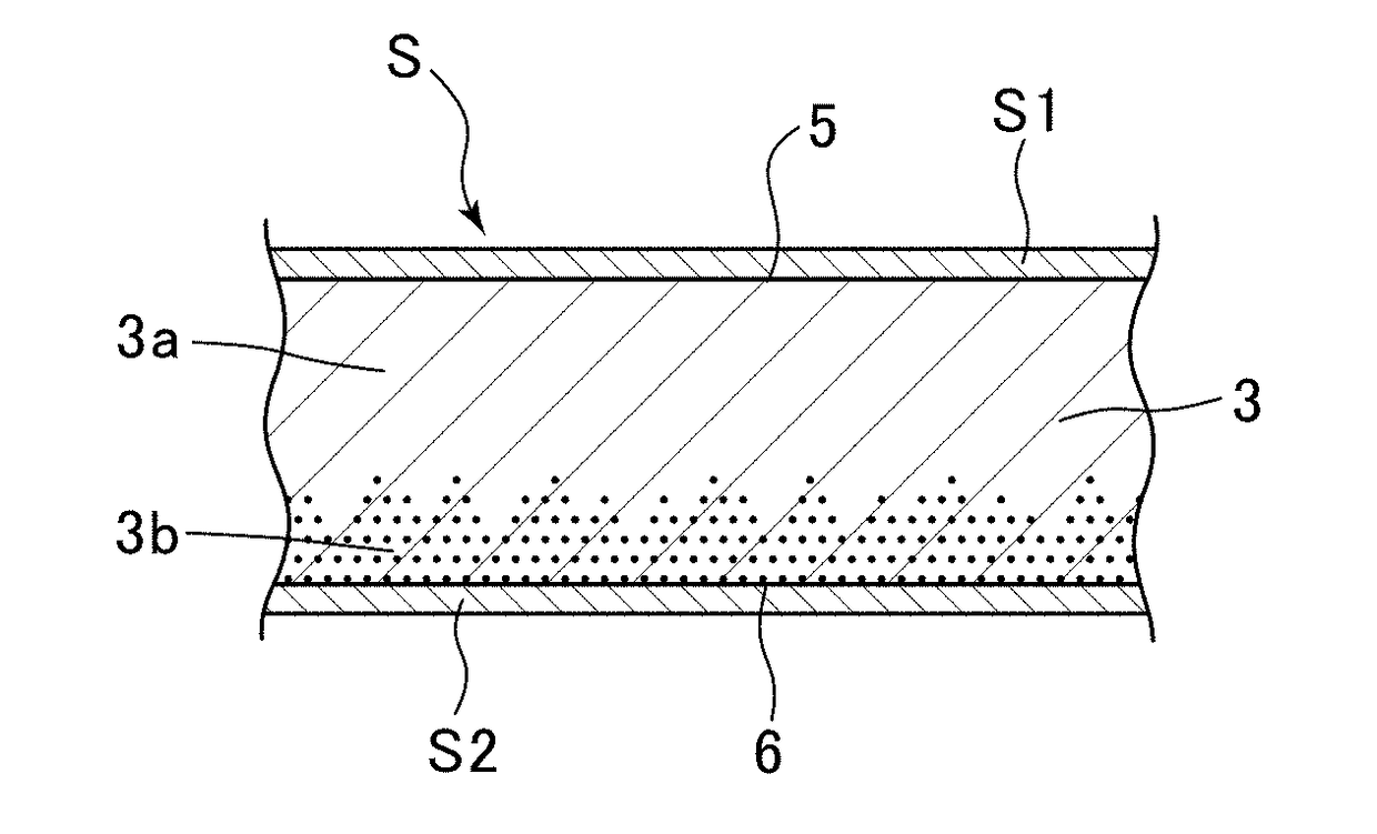
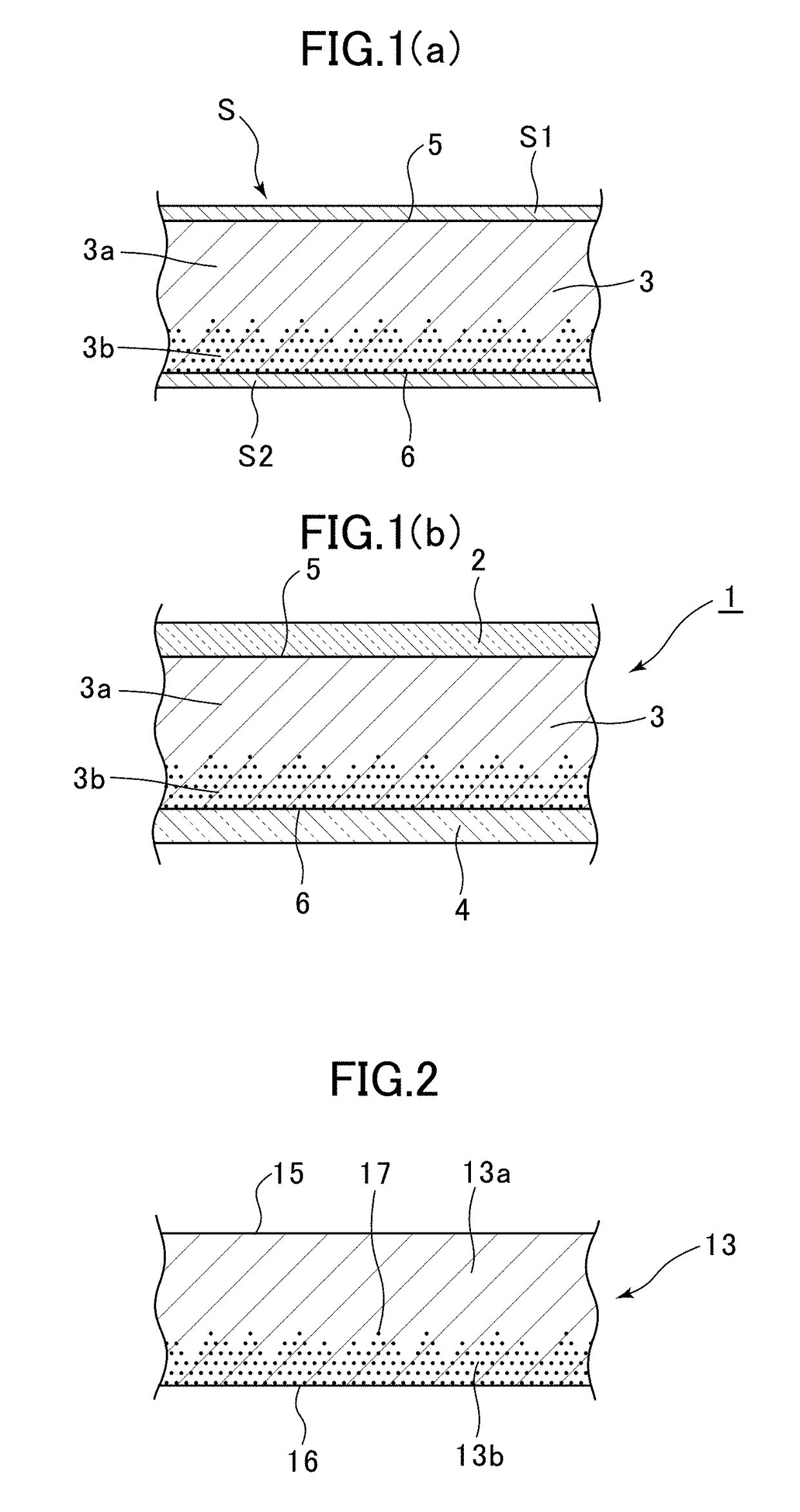
The present invention relates to a pressure-sensitive adhesive sheet used for bonding optical elements together. The sheet has a refractive index adjustment zone with a higher refractive index than the adhesive material, which can reduce reflected light and prevent interface reflection. The refractive index adjustment zone can be adjusted with respect to the refractive indexes of the optical elements and a patterned transparent electroconductive layer. The sheet can be preliminarily laminated with a substrate provided with an electroconductive layer, which simplifies handling and reduces process time and materials usage.

Problems solved by technology

This configuration involves a problem that, when outside light enters from the transparent optical element on the viewing side, the entered light is reflected at an interface between the pressure-sensitive adhesive layer and the optical element on a non-viewing side, and returned to the viewing side.
This problem becomes prominent particularly when an entry angle of outside light is relatively large.
In this type of display device, the problem “poor pattern invisibility” is pointed out that a pattern of the transparent electroconductive layer becomes visible from the viewing side, by the influence of internal reflection of entered light at an interface between a pressure-sensitive adhesive layer and the transparent electroconductive layer.
On the other hand, there is a problem that the composition itself becomes costly, because this technique is based on the use of a particular monomer component.
However, the technique disclosed in the Patent Document 2 requires using the high refractive index material in large amounts.
This causes a concern about deterioration in properties required as a pressure-sensitive adhesive, and a problem of an increase in cost.
Thus, there is another problem that the particles are hardly dispersed, causing whitish haze due to light scattering.
In this case, however, it becomes difficult to solve a problem of coloration.
However, it cannot solve most of the remaining problems pointed out in connection with the Patent Document 2.
Thus, the resulting pressure-sensitive adhesive becomes more costly than that in the Patent Document 2.

Method used


Image

  • Electroconductive film laminate comprising transparent pressure-sensitive adhesive layer
  • Electroconductive film laminate comprising transparent pressure-sensitive adhesive layer
  • Electroconductive film laminate comprising transparent pressure-sensitive adhesive layer

Examples


##ventive example 1

Inventive Example 1

[0119]Based on the method described in the aforementioned , an optical element laminate depicted in FIG. 8(a) was produced. The optical element laminate depicted in FIG. 8(a) was formed by: laminating the transparent electroconductive film (A) (laminate 21) to one surface of the pressure-sensitive adhesive-laminated transparent electroconductive film (1) (laminate 51) defined by the refractive index adjustment zone; laminating one surface of the refractive index adjustment zone-formed pressure-sensitive adhesive sheet (A1) defined by the refractive index adjustment zone, to the other surface of the pressure-sensitive adhesive-laminated transparent electroconductive film (1) (laminate 51) defined by the ITO layer; and laminating an evaluation ZEONOA 57 to the other surface of the refractive index adjustment zone-formed pressure-sensitive adhesive sheet (A1). Further, for reflectance measurement, an evaluation black PET film 58 was laminated to an outer surface of t...

##ventive example 2

Inventive Example 2

[0120]In the same manner as that in Inventive Example 1, an optical element laminate depicted in FIG. 8(b) was produced. The optical element laminate depicted in FIG. 8(b) was formed by: laminating the transparent electroconductive film (B) (laminate 31) to one surface of the pressure-sensitive adhesive-laminated transparent electroconductive film (2) (laminate 52) defined by the refractive index adjustment zone; laminating one surface of the refractive index adjustment zone-formed pressure-sensitive adhesive sheet (B1) defined by the refractive index adjustment zone, to the other surface of the pressure-sensitive adhesive-laminated transparent electroconductive film (2) (laminate 52) defined by the ITO layer; and laminating an evaluation ZEONOA 57 to the other surface of the refractive index adjustment zone-formed pressure-sensitive adhesive sheet (B1). Further, for reflectance measurement, an evaluation black PET film 58 was laminated to an outer surface of the ...

##ventive example 3

Inventive Example 3

[0121]In the same manner as that in Inventive Examples 1 and 2, an optical element laminate depicted in FIG. 8(c) was produced. The optical element laminate depicted in FIG. 8(c) was formed by: laminating the transparent electroconductive film (A) (laminate 21) to one surface of the pressure-sensitive adhesive-laminated transparent electroconductive film (3) (laminate 53) defined by the refractive index adjustment zone; laminating one surface of the refractive index adjustment zone-formed pressure-sensitive adhesive sheet (C1) defined by the refractive index adjustment zone, to the other surface of the pressure-sensitive adhesive-laminated transparent electroconductive film (3) (laminate 53) defined by the ITO layer; and laminating an evaluation ZEONOA 57 to the other surface of the refractive index adjustment zone-formed pressure-sensitive adhesive sheet (C1). Further, for reflectance measurement, an evaluation black PET film 58 was laminated to an outer surface ...


PUM

PropertyMeasurementUnit
thicknessaaaaaaaaaa
thicknessaaaaaaaaaa
refractive indexaaaaaaaaaa

Abstract

In the case where a pressure-sensitive adhesive sheet comprising a pressure-sensitive adhesive layer having a refractive index adjustment zone is provided in such a manner that two PET separators are laminated to opposite surfaces of the pressure-sensitive adhesive layer, it is difficult to distinguish between obverse and reverse sides of the pressure-sensitive adhesive sheet itself. The present invention is directed to solving the above problems and, specifically, to offering a pressure-sensitive adhesive sheet having a refractive index adjustment zone capable of being easily produced at low cost, in a state in which it is preliminarily laminated with a substrate provided with an electroconductive layer, thereby making it possible to resolve complexity in handling (to easily distinguish between one surface defined by the refractive index adjustment zone and the other surface defined by the remaining zone).

Description

TECHNICAL FIELD[0001]The present invention relates to an electroconductive film laminate comprising a transparent pressure-sensitive adhesive layer. In particular, the present invention relates to an electroconductive film laminate comprising a transparent electroconductive film to which a pressure-sensitive adhesive sheet comprising a pressure-sensitive adhesive layer capable of effectively suppressing internal reflection is laminated.BACKGROUND ART[0002]In a display device such as a liquid crystal display device or an organic EL display device, a pressure-sensitive adhesive is used to bond a transparent optical element, such as a polarizing film, a retardation film or a transparent cover element including a cover glass, to another optical element. That is, a pressure-sensitive adhesive layer is disposed between two optical elements to be bonded together, and then the two optical elements are pressed against each other and bonded together to thereby form an optical element laminate...

Claims


Application Information

Patent Timeline
Patent Type & Authority Applications(United States)
IPC IPC(8): B32B7/02H01B5/14C09J7/02B32B17/10B32B7/12H01B1/08
CPCB32B7/02B32B7/12B32B17/1055H01B5/14C09J7/02H01B1/08B32B2307/412B32B2315/08B32B2457/208B32B2386/00B32B2307/202G02B5/0215G02B5/0242B32B7/06B32B15/09B32B15/085B32B27/06B32B27/08B32B2250/02B32B2250/24B32B15/02B32B15/20B32B27/16B32B27/325B32B27/36B32B27/365B32B27/285B32B27/286B32B27/34B32B27/281B32B27/32B32B27/308B32B27/304B32B27/302B32B27/306B32B2255/26B32B2255/10B32B2255/20B32B2307/732B32B2307/748B32B2307/418B32B2405/00B32B2457/20B32B2457/202B32B2457/206B32B17/06C09J9/02C09J11/04
Inventor KATAMI, HIROFUMIUMEMOTO, TORUTAKAO, HIROYUKIYASUI, ATSUSHI
Owner NITTO DENKO CORP
Features
  • R&D
  • Intellectual Property
  • Life Sciences
  • Materials
  • Tech Scout
  • Unparalleled Data Quality
  • Higher Quality Content
  • 60% Fewer Hallucinations
Learn More