Hold checking method and unhold checking method for wafer

a technology of unhold checking and wafer, which is applied in electrical devices, semiconductor/solid-state device testing/measurement, electrical discharge tubes, etc., can solve the problems of difficult to reliably hold the wafer on the chuck table under vacuum chamber suction, not easy to check whether or not the wafer is sufficiently held by the electrostatic chuck, and the possibility of arcing (abnormal discharge) or tape burning caused

Active Publication Date: 2018-01-25
DISCO CORP
View PDF4 Cites 8 Cited by
  • Summary
  • Abstract
  • Description
  • Claims
  • Application Information

AI Technical Summary

Benefits of technology

[0014]According to the hold checking method of the present invention, the following effect can be obtained. Even in the case that wafer is loaded to the electrostatic chuck included in the vacuum processing apparatus, that is, even in the case that it is difficult for a processing apparatus to determine whether or not the wafer is sufficiently held by the electrostatic chuck, the vacuum processing apparatus according to the present invention can easily determine whether or not the wafer is sufficiently held by the electrostatic chuck.
[0015]...

Problems solved by technology

In the case that a chuck table for holding the wafer is of a type such that the wafer is held under suction on the chuck table, it is difficult to reliably hold the wafer on the chuck table under suction in the vacuum chamber evacuated.
In contrast, in the case that the wafer is held by the electrostatic chuck provided in the enclosed and evacuated vacuum chamber in the plasma etching apparatus, it is not easy to check whether or not the wafer is sufficiently held by the electrostatic chuck.
If plasma etching is started in the condition where the wafer is not sufficiently held by the electrostatic chuck, the...

Method used


Image

  • Hold checking method and unhold checking method for wafer
  • Hold checking method and unhold checking method for wafer
  • Hold checking method and unhold checking method for wafer

Examples


Embodiment Construction

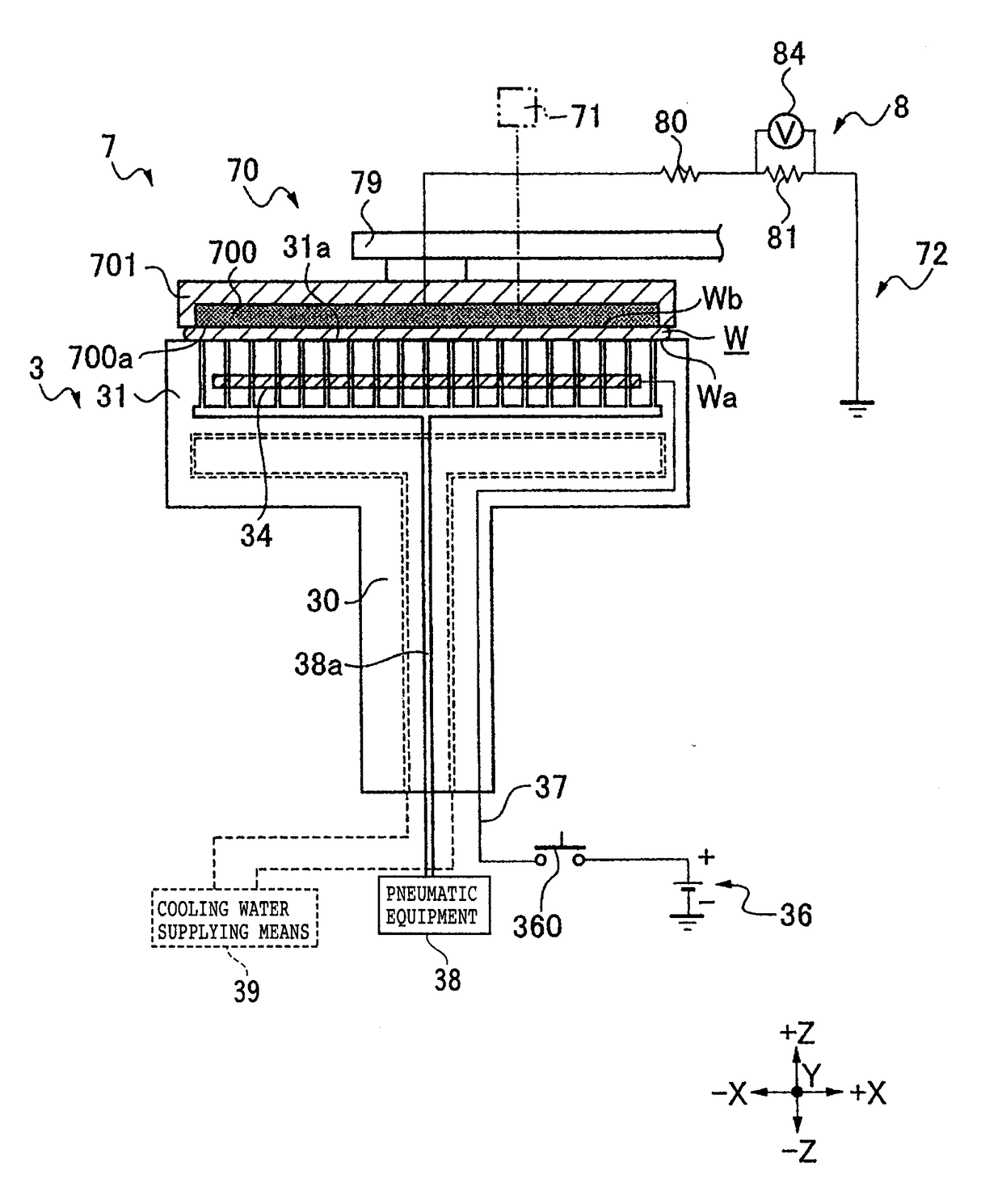
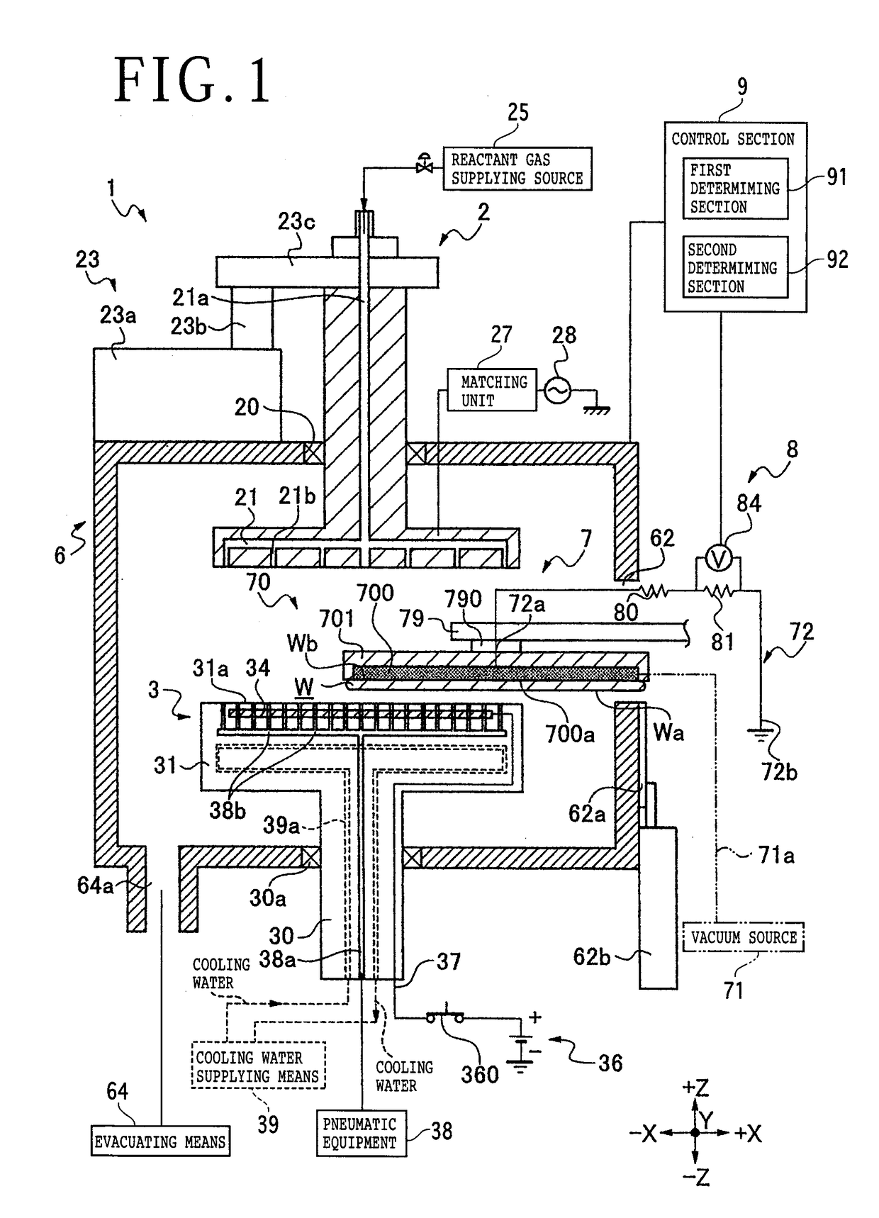
[0023]Referring to FIG. 1, there is depicted a vacuum processing apparatus 1 for processing a wafer W in a vacuum environment (under a reduced pressure). The vacuum processing apparatus 1 depicted in FIG. 1 is a plasma etching apparatus including an electrostatic chuck 3 having a holding surface 31a for holding the wafer W, a vacuum chamber 6 equipped with evacuating means 64 for evacuating the inside space of the vacuum chamber 6 in which the electrostatic chuck 3 is provided, and transfer means 7 for loading the wafer W into the vacuum chamber 6 and unloading the wafer W out of the vacuum chamber 6. The vacuum processing apparatus 1 according to the present invention is not limited to such a plasma etching apparatus.

[0024]The electrostatic chuck 3 includes a shaft portion 30 rotatably supported through a bearing 30a to a lower portion of the vacuum chamber 6 and a wafer holding portion 31 formed of a dielectric such as ceramic (e.g., alumina and titanium oxide). As depicted in FIG...


PUM


Abstract

Disclosed herein is a hold checking method for checking whether or not a wafer is held by an electrostatic chuck in loading the wafer to the electrostatic chuck by operating a transfer unit holding the wafer. The hold checking method includes a connecting step of bringing the wafer held by a transfer pad into contact with the electrostatic chuck to thereby connect the transfer pad through the wafer to the electrostatic chuck, and a hold determining step of supplying electric power from a DC power source through first wiring to the electrostatic chuck after performing the connecting step, and next determining that the wafer is held by the electrostatic chuck when the voltage across a resistor inserted in the first wiring has reached a predetermined voltage value.

Description

BACKGROUND OF THE INVENTIONField of the Invention[0001]The present invention relates to a hold checking method for checking whether or not a wafer is held by an electrostatic chuck, an unhold checking method for checking whether or not the wafer is unheld from the electrostatic chuck, and a vacuum processing apparatus for processing the wafer in a vacuum environment.Description of the Related Art[0002]A wafer such as a semiconductor wafer is ground by a grinding apparatus to reduce the thickness of the wafer to a predetermined thickness. Thereafter, the wafer is divided into individual device chips by using a cutting apparatus, for example. The device chips are used in various electronic equipment or the like. In grinding the wafer, a protective tape is previously attached to the front side of the wafer on which a plurality of devices are formed. The wafer is held on a holding table in the condition where the protective tape attached to the front side of the wafer is in contact with...

Claims


Application Information

Patent Timeline
IPC IPC(8): H01L21/67H01L21/677H01J37/32H01L21/683
CPCH01L21/67259H01L21/6833H01L21/67742H01J2237/334H01J37/32009H01J37/32697H01L21/67069H01J37/32733H01J37/32935H01L21/6831H01J37/32715H01L22/14H01L21/67739H01L21/67242
Inventor CHITO, KENTA
Owner DISCO CORP
Why Eureka
Try Eureka