Location-Specific Tuning of Stress to Control Bow to Control Overlay In Semiconductor Processing

a technology of stress and location, applied in the direction of semiconductor/solid-state device testing/measurement, image enhancement, instruments, etc., can solve the problems of overlay errors, expansion exceeds overlay error tolerances, and larger overlay errors

Active Publication Date: 2018-03-08
TOKYO ELECTRON LTD
View PDF6 Cites 17 Cited by
  • Summary
  • Abstract
  • Description
  • Claims
  • Application Information

AI Technical Summary

Benefits of technology

[0011]Note that this summary section does not specify every embodiment and/or incrementally novel aspect of the present disclosure or claimed invention. Instead, this summary only provides a preliminary discussion of different embodiments and corresponding points

Problems solved by technology

An error in overlay means that a layer is offset with respect to a layer below (or above) it.
Any movement of the substrate relative to the substrate stage after alignment, however, can result in overlay errors.
If the substrate expansion is unchecked, the expansion exceeds overlay error tolerances.
Moreover, if the clamping force between the substrate and the substrate chuck is not sufficient to prevent substrate expansion, then the substrate can slip on the substrate chuck and larger substrate expansion will occur, resulting in larger overlay errors.
Thus, vacuum clamping is not always possible, and the weaker electrostatic clamping must be used in lieu of a vacuum clamp.
Other fabrication steps can also cause substrate expansion and contraction.
For example, deposited films can cause

Method used


Image

  • Location-Specific Tuning of Stress to Control Bow to Control Overlay In Semiconductor Processing
  • Location-Specific Tuning of Stress to Control Bow to Control Overlay In Semiconductor Processing
  • Location-Specific Tuning of Stress to Control Bow to Control Overlay In Semiconductor Processing

Examples


Embodiment Construction

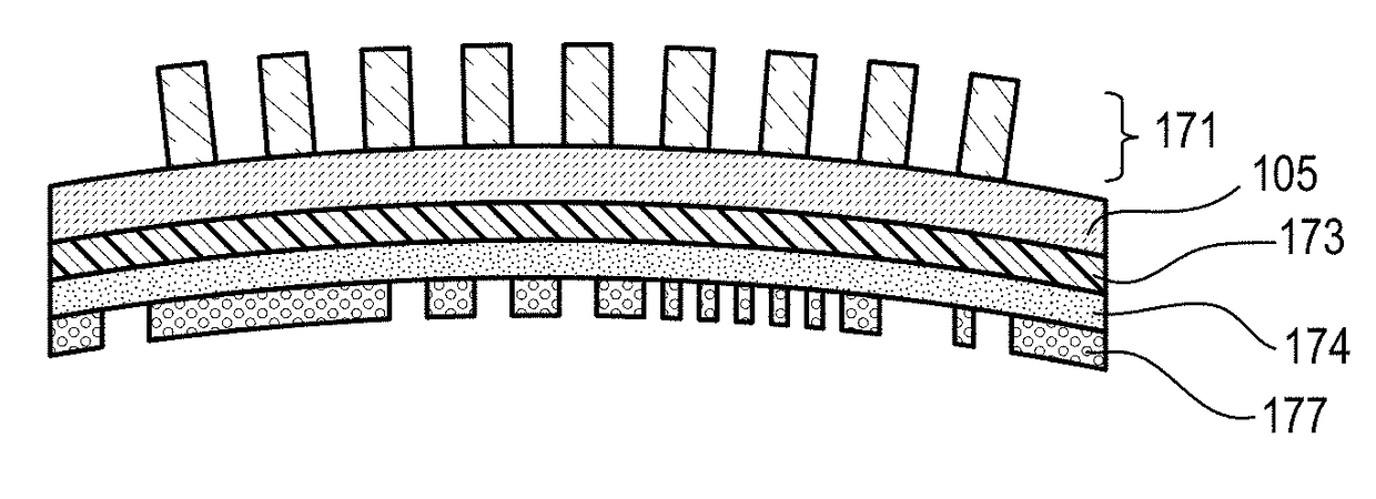
[0030]Techniques herein include systems and methods for correcting pattern overlay errors by correcting or adjusting bowing of semiconductor substrates (wafers). Techniques herein include systems and methods for location-specific tuning of stress on wafers to reduce overlay error. Location-specific tuning of stress independently modifies specific regions, areas, or point locations on a substrate to change wafer bow at those specific locations. Such spatial stress tuning with differential control reduces overlay error on substrates, which in turn improves overlay of subsequent patterns created on the substrate. Techniques herein include receiving a substrate with some amount of overlay error, measuring bow of the substrate to map z-height deviations across the substrate, generating an overlay correction pattern, and then physically modifying internal stresses on the substrate at specific locations with these modifications and intensities being independent of other locations. Such mod...


PUM


Abstract

Techniques herein include systems and methods for correcting pattern overlay errors by correcting or adjusting bowing of wafers. Location-specific tuning of stress on semiconductor substrates reduces overlay error. Location-specific tuning of stress independently modifies specific regions, areas, or point locations on a substrate to change wafer bow at those specific locations, which reduces overlay error on substrates, which in turn improves overlay of subsequent patterns created on the substrate. Techniques herein include receiving a substrate with some amount of overlay error, measuring bow of the substrate to map z-height deviations across the substrate, generating an overlay correction pattern, and then physically modifying internal stresses on the substrate at specific locations with modifications independent of other coordinate locations. Such modifications can include etching a backside surface of the substrate. One or more processing modules can be used for such processing.

Description

CROSS REFERENCE TO RELATED APPLICATIONS[0001]The present application claims the benefit of U.S. Provisional Patent Application No. 62 / 383,549, filed on Sep. 5, 2016, entitled “Method for Correcting Wafer Bow,” which is incorporated herein by reference in its entirety.BACKGROUND OF THE INVENTION[0002]This disclosure relates to semiconductor fabrication, and particularly to wafer overlay.[0003]Semiconductor fabrication involves multiple varied steps and processes. One typical fabrication process is known as photolithography (also called microlithography). Photolithography uses radiation, such as ultraviolet or visible light, to generate fine patterns in a semiconductor device design. Many types of semiconductor devices, such as diodes, transistors, and integrated circuits, can be constructed using semiconductor fabrication techniques including photolithography, etching, film deposition, surface cleaning, metallization, and so forth.[0004]Exposure systems (also called tools) are used t...

Claims


Application Information

Patent Timeline
IPC IPC(8): H01L21/302H01L21/66H01L21/027G03F7/20
CPCH01L21/302H01L22/20H01L22/12H01L22/30H01L21/027G03F7/70633H01L21/68G03F7/70783H01L21/0274H01L21/67115H01L21/6715H01L21/67288H01L21/6875G06F30/23H01L22/32H01L22/26H01L21/67259H01L21/67253G06F30/20G06T7/0004G06T2207/30148G03F7/70525
Inventor DEVILLIERS, ANTON J.
Owner TOKYO ELECTRON LTD
Why Eureka
Try Eureka