Self-aligned optical grid on image sensor

Active Publication Date: 2018-03-29
OMNIVISION TECH INC
View PDF1 Cites 3 Cited by
  • Summary
  • Abstract
  • Description
  • Claims
  • Application Information

AI Technical Summary

Benefits of technology

[0008]The present invention overcomes the problems associated with the prior art by providing an image capture device with reflective walls disposed between adjacent color filters. A method of forming the reflective sid

Problems solved by technology

Crosstalk between pixels (e.g., light filtered by one pixel but measured by another, differently colored pixel) diminishes the accuracy of measurement and causes undesirable distortions in the colors of the captured images.
The opaque spacer significantly decreases crosstalk between adjacent pixels, but is approximately 50 nm thick and, therefore, reduces the quantum efficiency (QE) of each pixel.
However, the sidewall of Qian et al. also reduces QE, because the sidewall is dark and absorbs incident light.
Because some of the light incident on each pixel is absorbed, the sensitivity of the pixels is diminis

Method used


Image

  • Self-aligned optical grid on image sensor
  • Self-aligned optical grid on image sensor
  • Self-aligned optical grid on image sensor

Examples


Example

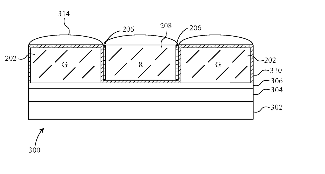
[0026]The present invention overcomes the problems associated with the prior art, by providing an image sensor including a reflective sidewall between adjacent color filters and methods of producing the same. In the following description, numerous specific details are set forth (e.g., layout of color filters, semiconductor fab processes, etc.) in order to provide a thorough understanding of the invention. Those skilled in the art will recognize, however, that the invention may be practiced apart from these specific details. In other instances, details of well-known image sensor production practices (e.g., etching, doping, chemical / physical vapor deposition, routine optimization, etc.) and components have been omitted, so as not to unnecessarily obscure the present invention.

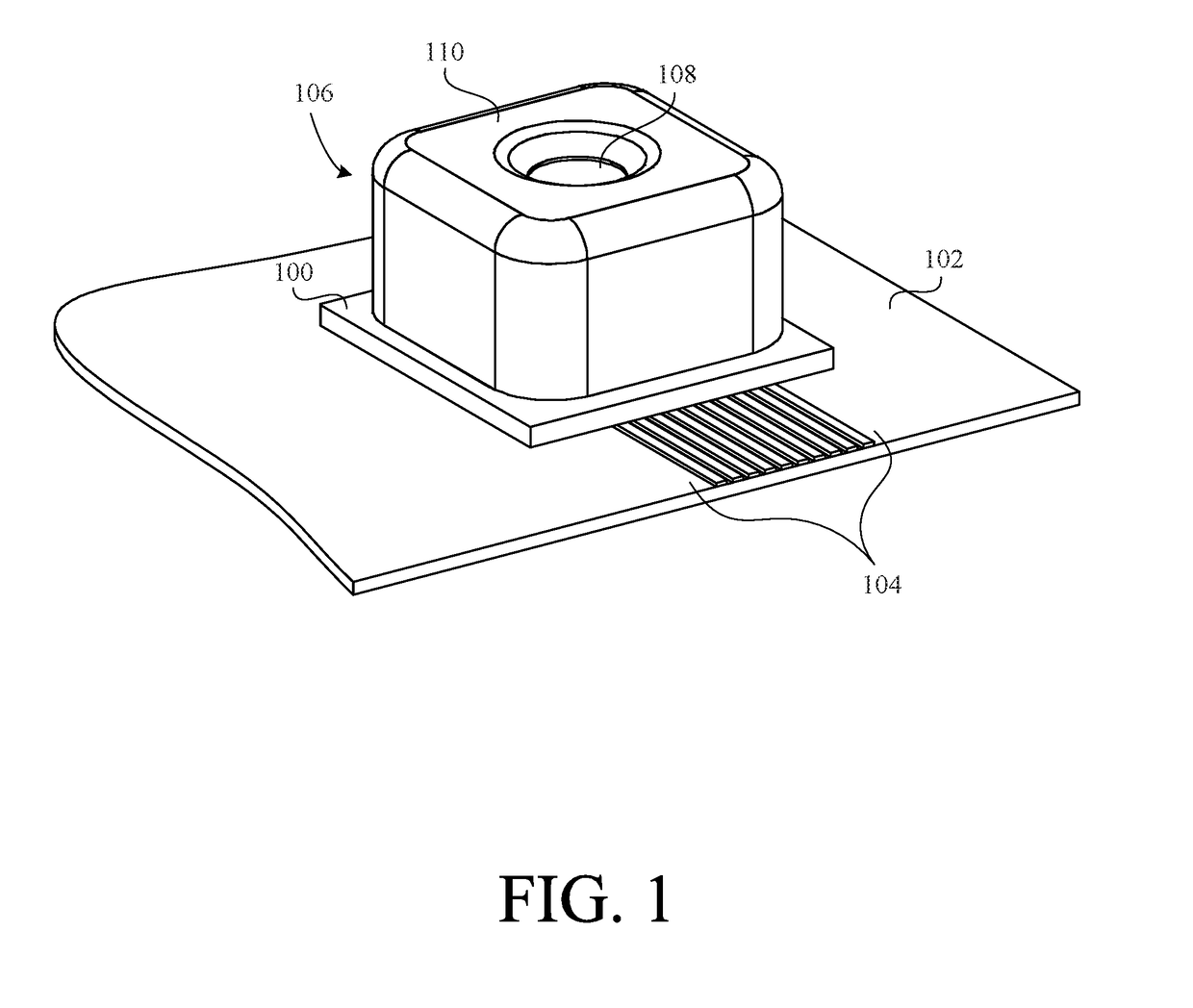
[0027]FIG. 1 is a perspective view of an image sensor 100 mounted on a portion of a printed circuit board (PCB) 102 that represents a PCB of a camera hosting device (e.g., automobile, manufacturing machine, medic...


PUM


Abstract

An image sensor includes a substrate, a plurality of light sensitive pixels, a first plurality of color filters, a plurality of reflective sidewalls, and a second plurality of color filters. The light sensitive pixels are formed on said substrate. The first plurality of color filters is disposed over a first group of the light sensitive pixels. The reflective sidewalls are formed on each side of each of the first plurality of color filters. The second plurality of color filters are disposed over a second group of light sensitive pixels and each color filter of the second plurality of color filters is separated from each adjacent filter of said first plurality of color filters by one of the reflective sidewalls. In a particular embodiment an etch-resistant layer is disposed over the first plurality of color filters and the second group of light sensitive pixels.

Description

BACKGROUND OF THE INVENTIONField of the Invention[0001]This invention relates generally to color image sensors. More particularly, it relates to image sensors having a light filter array with an optical grid for minimizing pixel cross-talk.Description of the Background Art[0002]Image sensors that are able to capture colored images are well known in the prior art. Such image sensors include a plurality of light sensitive regions (e.g. photodiodes) and a plurality of variously colored light filters. Each pixel includes a light filter of a single color disposed over the photodiode, which is connected to readout circuitry for determining the amount of light (within the spectrum corresponding to the color of the light filter) that impinges on the pixel during a shutter period. The pixels are typically arranged in rows and columns, with a red pixel (i.e. one having a color filter adapted to pass red light), a blue pixel, and two green pixels making up each 2×2 square of pixels (i.e. a Bay...

Claims


Application Information

Patent Timeline
IPC IPC(8): H01L27/146
CPCH01L27/14685H01L27/14629H01L27/14621
Inventor WANG, XINYANG, DAJIANGWANG, QINMAO, DULITAI, DYSON HSIN-CHIH
Owner OMNIVISION TECH INC
Why Eureka
Try Eureka