Laser lift-off method of wafer

a technology of laser lift-off and wafer, which is applied in the field of laser microprocessing, can solve the problems of wasting materials, affecting the quality of finished products, and a greater risk of process scrapping in the whole silicon ingot process, and achieves the effects of high process yield, high efficiency and convenient mass production

a technology of laser lift-off and wafer, which is applied in the field of laser microprocessing, can solve the problems of wasting materials, affecting the quality of finished products, and a greater risk of process scrapping in the whole silicon ingot process, and achieves the effects of high process yield, high efficiency and convenient mass production

US20180108568A1Active Publication Date: 2018-04-19HANS LASER TECH IND GRP CO LTD

Image

  • Laser lift-off method of wafer
  • Laser lift-off method of wafer
  • Laser lift-off method of wafer

Examples


Embodiment Construction

[0011]The foregoing and other objects, features and advantages will be apparent from the following description of particular embodiments of the invention, as illustrated in the accompanying drawings. It should be noted that, the specific embodiment illustrated herein is merely for the purpose of illustration, and should not be deemed to limit the invention.

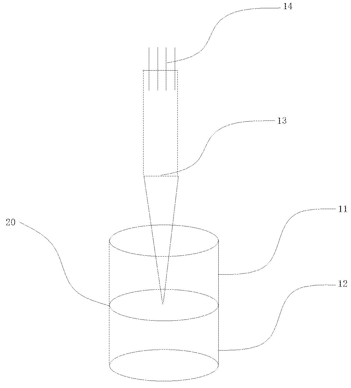
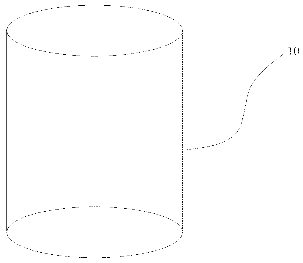
[0012]As shown in FIG. 1, a laser lift-off method of a silicon wafer 10 according to an embodiment includes the following steps:

[0013]In step S110, a laser is focused to an inside of a silicon wafer to form a plurality of cracking points, the plurality of cracking points are located on a separating surface. Specifically, the laser is focused on a flat surface in the silicon wafer to form a plurality of cracking points. For example, the plurality of cracking points are located on a same flat surface, the flat surface is the separating surface. For example, the plurality of cracking points are not located on a same flat surface, thu...


PUM

PropertyMeasurementUnit
distanceaaaaaaaaaa
thicknessaaaaaaaaaa
diameteraaaaaaaaaa

Abstract

The present invention relates to a laser lift-off method of wafer. The method includes the steps as follows: focusing laser in an inside for a wafer (10) to form a plurality of cracking points (19), the plurality of cracking points (19) are located on a separating surface (20); and exerting, under a temperature of −400K to 0K, forces with opposite directions to opposite sides of the wafer (10), thereby dividing the wafer (10) into two pieces along the separating surface (20).

Description

FIELD OF THE INVENTION[0001]The present disclosure relates to a field of laser micro-processing, and more particularly relates to a laser lift-off method for a wafer.BACKGROUND OF THE INVENTION[0002]In the industry of silicon wafer semiconductor, in order to obtain a single silicon wafer having a relative less thickness, at present, the conventional processing method is to cut the crystal bar by a wire-electrode cutting method first, and then the crystal bar is grinded and thinned to a predetermined thickness. The disadvantage of the processing method is wasting material; quite a lot of silicon wafer is grinded in the grinding process, thus causing a loss of materials.[0003]Due to a development of the semiconductor industry and a continuous promotion of a consciousness of energy conservation and environment protection, a more scientific and lossless processing method is to be developed, a laser lift-off technology is initially applied to the silicon wafer lift-off industry, but the ...

Claims


Application Information

Patent Timeline
19 Apr 2018
Publication
US20180108568A1
IPC
H01L21/78; B23K26/00; B23K26/02
CPC
H01L21/7813; B23K26/0057; B23K26/02; B23K2201/40; H01L31/18; B23K26/0006; B23K26/38; B23K26/402
Inventors
WANG, YANHUA; ZHUANG, CHANGHUI