Field Programmable Gate Array

Active Publication Date: 2018-04-26
HITACHI LTD
View PDF6 Cites 3 Cited by
  • Summary
  • Abstract
  • Description
  • Claims
  • Application Information

AI Technical Summary

Benefits of technology

[0020]According to the invention, it is possible to provide a field programmable gate array which is able to prevent an inappropriate value from being output to the outside of an FPGA even when an SRAM-based programmable logic (herein

Problems solved by technology

In the worst case, a failure or an abnormality may occur in a system, and thus there is a need to take an action not to make the system out of control and fall into a dangerous state.
However, in recent years, a production cost of the ASIC is increased as a semiconductor process is departmentalized, and thus it is difficult to develop a new product in an industrial control system of which

Method used


Image

  • Field Programmable Gate Array
  • Field Programmable Gate Array
  • Field Programmable Gate Array

Examples


first embodiment

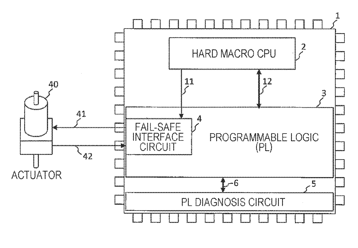
[0036]FIG. 1 is a diagram illustrating an example of a field programmable gate array (FPGA) of the invention.

[0037]The FPGA (1) has therein a hard macro CPU (2) in which the circuit configuration is fixed and the function is not changeable, a programmable logic (PL) 3 in which the circuit configuration is changeable at the time of power activation or in operation, a fail-safe (FS) interface circuit 4 which is configured in the PL (3), and a PL diagnosis circuit 5.

[0038]The hard macro CPU (2) is mounted to output a unidirectional FS control signal 11 to the FS interface circuit 4, and a bidirectional PL control signal 12 is output from the hard macro CPU (2) with respect to the PL (3).

[0039]In addition, the PL diagnosis circuit 5 is a diagnosis circuit which can detect a failure or an error in a case where the failure or the error occurs in the PL (3), and is connected to the PL (3) through a PL diagnosis signal 6 to exchange information necessary for the diagnosis. In this embodimen...

second embodiment

[0060]Next, the description will be given about an example of the system using the FPGA of the invention in which a higher safety is realized.

[0061]FIG. 7(a) is a timing chart illustrating an example of a starting-up process of the system using the FPGA of the invention, in which it is considered that the system operates in a control period with the same contents as those illustrated in the timing chart of FIG. 6 of the first embodiment.

[0062]In the system, as illustrated in FIG. 7(a), the starting-up process is performed after power is input and then an FS output start process 55 is first performed before the procedure enters a normal process by a control period, and the system becomes a state in which a signal indicating FS is output to a device connected to the FPGA.

[0063]After the FS output start process 55, a start process 56 is performed and minimum resources necessary for the system to operate are activated. Then, when the diagnosis of the PL is normally ended by the PL diagn...

third embodiment

[0066]Next, the description will be given about an example in a case where an FS configuration is realized not to output erroneous data to the outside of the FPGA of the invention.

[0067]FIG. 8 illustrates an example of four types of FS signals which are output from the FS interface circuit in the FPGA in synchronization with a clock signal.

[0068]FIG. 8(a) illustrates an example in a case where an FS signal is output which becomes a high potential (High) when a failure or an error occurs in the system. Herein, when an error is detected in the FPGA at a clock cycle c2, the High signal is output as the FS signal after a clock cycle c3.

[0069]FIG. 8(b) illustrates an example in a case where an FS signal is output which becomes a low potential (Low) when a failure or an error occurs in the system in contrast to FIG. 8(a). Herein, when an error is detected in the FPGA at the clock cycle c2, the Low signal is continuously output as the FS signal after the clock cycle c3.

[0070]FIG. 8(c) illu...


PUM


Abstract

An object of the invention is to provide a field programmable gate array which is able to prevent an inappropriate value from being output to the outside of an FPGA even when an SRAM-based programmable logic portion is out of order and to secure safety of a system. The field programmable gate array of the invention includes a hard macro CPU in which a circuit structure is fixed, a programmable logic in which a circuit structure is changeable, a diagnosis circuit which diagnoses an abnormality of the programmable logic, and a fail-safe interface circuit which is able to control an external output from the programmable logic to a safe side, and the hard macro CPU outputs a fail-safe signal which is an output of a safe side to the fail-sate interface circuit when an error is detected by the diagnosis circuit.

Description

TECHNICAL FIELD[0001]The invention relates to a field programmable gate array.BACKGROUND ART[0002]In a control system where an extremely high reliability is required to secure safety in human life and environment such as a plant, a railway, a vehicle, and an airplane. In the worst case, a failure or an abnormality may occur in a system, and thus there is a need to take an action not to make the system out of control and fall into a dangerous state.[0003]Therefore, a lot of reliability and safety is required in a control device which performs control in the system.[0004]Until now, an ASIC (Application Specific Integrated Circuit) has been mainly used in the control of such a control device.[0005]However, in recent years, a production cost of the ASIC is increased as a semiconductor process is departmentalized, and thus it is difficult to develop a new product in an industrial control system of which the number of production is less.[0006]On the other hand, a field programmable gate a...

Claims


Application Information

Patent Timeline
IPC IPC(8): G06F11/08H03K19/177G01R31/3185
CPCG06F11/085H03K19/17776H03K19/17728H03K19/17744H03K19/1776G01R31/318519B61L5/18G06F11/1004H03K19/17758H03K19/173
Inventor SAKATA, TERUAKIYAMADA, TSUTOMU
Owner HITACHI LTD
Why Eureka
Try Eureka