Method and system for building a cell library with segmented timing arc delay model

Inactive Publication Date: 2018-05-17
JOO BYUNGHA
View PDF16 Cites 2 Cited by
  • Summary
  • Abstract
  • Description
  • Claims
  • Application Information

AI Technical Summary

Benefits of technology

[0010]To improve gate delay accuracy without unduly increasing cell library size and analytical complexity, the definition of propagation delay is not modified. In the present disclosure, propagation delay of a given logic gate is referenced from a logical threshold voltage level ½VDD while parasitic wire RC models are calculated in the conventional passive element timing model. However, the logic gate is no longer a black boxed. In the present invention, propagation delay from input to output is divided into multiple timing arcs

Problems solved by technology

However, the logic gate i

Method used


Image

  • Method and system for building a cell library with segmented timing arc delay model
  • Method and system for building a cell library with segmented timing arc delay model
  • Method and system for building a cell library with segmented timing arc delay model

Examples


Embodiment Construction

[0020]In the following detailed description, reference will be made to the accompanying drawings. The aforementioned accompanying drawings show by way of illustration, and not by way of limitation, specific embodiments and implementations consistent with the principles of the present invention. These implementations are described in sufficient detail to enable those skilled in the art to practice the invention, and it is to be understood that other implementations may be utilized and that structural changes and / or substitutions of various elements may be made without departing from the scope and spirit of the invention.

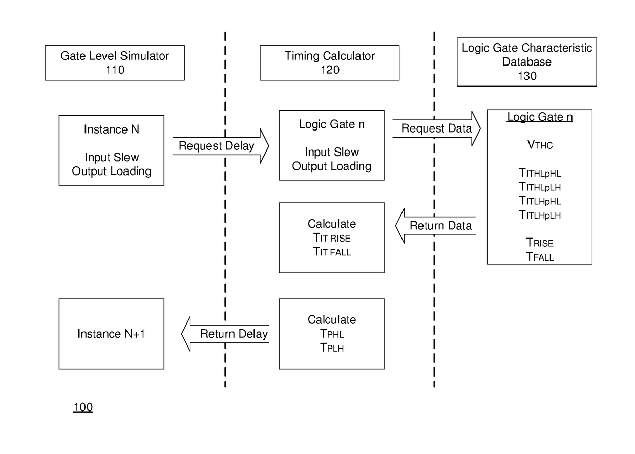
[0021]FIG. 2 is a schematic block diagram of a computer system adapted to use the segmented propagation delay model, according to an embodiment of the present disclosure. Referring to FIG. 2, gate level simulator 110 has a list of instances in a given design netlist. For each instance in the netlist, the gate level simulator 110 requests the timing calculator 120 for ...


PUM


Abstract

Multiple timing arc gate delay modelling method is described. Propagation delay can be divided into several timing arcs at circuit threshold voltage. Additionally, each timing arc can be modelled as a function of actual source of driving force. The logic threshold voltage of the functional gates is one single voltage level, which is usually half of the supplied voltage. Therefore, the RC tree model which is extracted from the wires is still valid. In this way, precise voltage based delay calculation is accomplished while maintaining the same interfacing method with passive RC elements from wirings.

Description

FIELD OF THE INVENTION[0001]The invention is in the field of electronic design automation (EDA), and more particularly, is related to system and method to enable accurate timing analysis of logical gates in a VLSI chip design.BACKGROUND OF THE INVENTION[0002]Timing analysis is one of key verification steps in every design flow for VLSI chips. Accurate delay modeling is increasingly becoming an important aspect of a VLSI chip design as the complexity of chips increases. In the past, higher throughput was the priority in designing VLSI chips. The art of VLSI chip design has evolved, and now, the power efficiency of the VLSI chip has become the one of the most important design goals, especially for mobile applications. This power and performance co-optimization can be achieved by maximizing utility of a clock period with useful data transactions. In other words, minimizing redundant timing margins in a clock period can eliminate waste of resource in designing of a VLSI chip. The precis...

Claims


Application Information

Patent Timeline
IPC IPC(8): G06F17/50
CPCG06F17/5031G06F30/327G06F30/3312G06F30/367G06F2119/12
Inventor JOO, BYUNGHA
Owner JOO BYUNGHA
Why Eureka
Try Eureka