Dynamic random access memory and fabrication method thereof

a random access memory and dynamic technology, applied in the field of dynamic random access memory (dram) and its fabrication, can solve the problem of complicated fabrication process of existing dram

Active Publication Date: 2018-05-17
SEMICON MFG INT (SHANGHAI) CORP +1
View PDF1 Cites 2 Cited by
  • Summary
  • Abstract
  • Description
  • Claims
  • Application Information

AI Technical Summary

Benefits of technology

The patent describes methods for making a memory structure in a semiconductor device. This structure can be formed during the fabrication process of other CMOS devices and can be connected to the device's select transistor without using a separate interconnect structure. This simplifies the fabrication process of the DRAM and reduces the complexity of the overall device. The technical effect of this patent is to provide a more efficient and simplified method for making DRAM arrays.

Problems solved by technology

However, the fabrication process of the existing DRAM is complicated.

Method used


Image

  • Dynamic random access memory and fabrication method thereof
  • Dynamic random access memory and fabrication method thereof
  • Dynamic random access memory and fabrication method thereof

Examples


Embodiment Construction

[0015]Reference will now be made in detail to exemplary embodiments of the disclosure, which are illustrated in the accompanying drawings. Wherever possible, the same reference numbers will be used throughout the drawings to refer to the same or like parts.

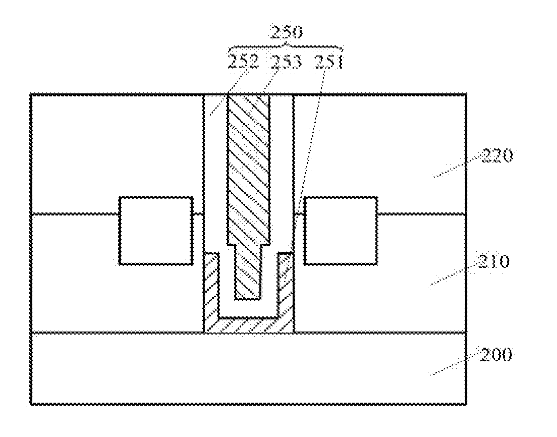
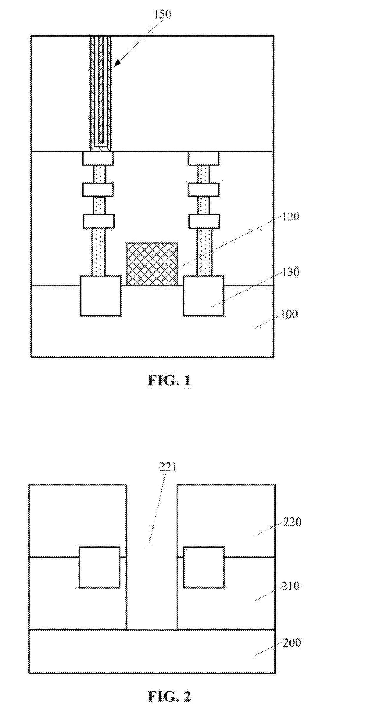
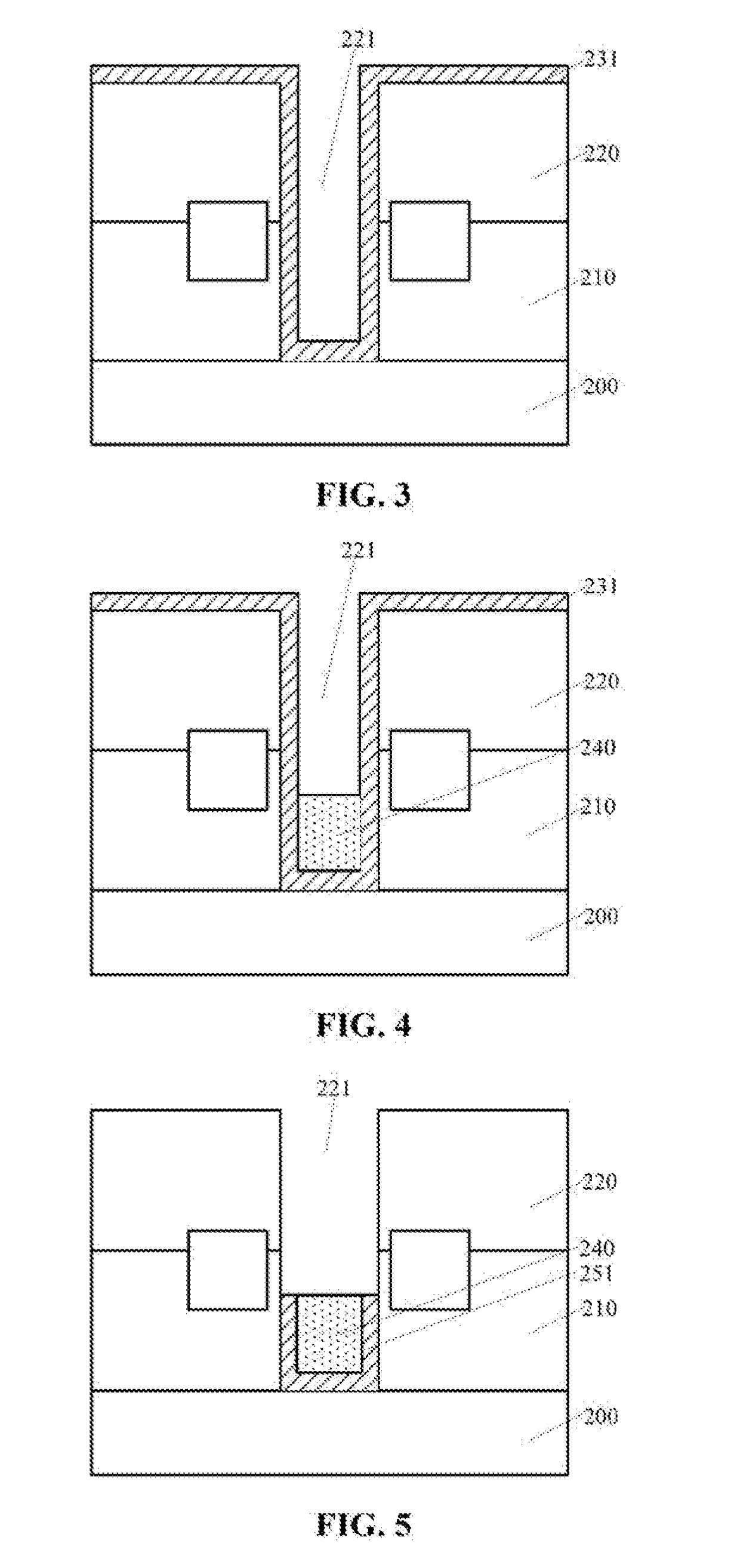
[0016]FIG. 1 illustrates a DRAM. As shown in FIG. 1, the DRAM includes a semiconductor substrate 100; a select transistor (not labeled) formed on the semiconductor substrate 100; an interconnect structure (not labeled) formed on the select transistor; a dielectric layer (not labeled) formed on the interconnect structure; a trench (not labeled) passing through the interlayer dielectric layer and exposing the top surface of the interconnect structure formed in the interlayer dielectric layer; and a capacitor (memory) structure 150 formed in the trench.

[0017]The capacitor structure 150 includes a first conductive layer formed on the side and bottom surfaces of the trench; a memory medium layer formed on the first conductive layer; an...


PUM


Abstract

Dynamic random access memory (DRAM) and fabrication methods thereof are provided. An exemplary fabrication method includes providing a base substrate; forming an interlayer dielectric layer over the base substrate; forming an opening passing through the interlayer dielectric layer; and forming a memory structure, having a first conductive layer, a memory medium layer on the first conductive layer, and a second conductive layer on the memory medium layer, in the opening.

Description

CROSS-REFERENCES TO RELATED APPLICATIONS[0001]This application claims the priority of Chinese patent application No. 201610994448.9, filed on Nov. 11, 2016, the entirety of which is incorporated herein by reference.FIELD OF THE DISCLOSURE[0002]The present disclosure generally relates to the field of semiconductor manufacturing technologies and, more particularly, relates to dynamic random access memory (DRAM) and fabrication methods thereof.BACKGROUND[0003]Dynamic random access memory (DRAM) often includes a memory cell, including a memory capacitor, and a transistor connected with the memory capacitor. The memory capacitor is used to store data; and the transistor is used to control the data storage of the memory capacitor.[0004]The working mechanism of the DRAM is as the following. The word line of the DRAM is electrically connected to the gate of the transistor in the memory cell to control the “on / off” of the transistor. The source of the DRAM is electrically connected to the so...

Claims


Application Information

Patent Timeline
Patent Type & Authority Applications(United States)
IPC IPC(8): H01L27/108H01L27/24H10N97/00H10N99/00
CPCH01L27/10879H01L27/10826H01L27/2436H10B12/00H10B12/30H10B12/02H10B12/37H10B12/01H01L28/92H10B63/30H10N70/231H10N70/20H10N70/8265H10N70/011H10B12/36H10B12/056
Inventor LIN, XISHEN, YI HUA
Owner SEMICON MFG INT (SHANGHAI) CORP
Why Eureka
Try Eureka