Integrated electroacoustic MEMS transducer with improved sensitivity and manufacturing process thereof

a technology of electroacoustic mems and transducers, applied in piezoelectric/electrostrictive devices, chemical vapor deposition coatings, decorative arts, etc., can solve the problem of further affecting the b>1/b> of the transducer

Active Publication Date: 2018-05-31
STMICROELECTRONICS SRL
View PDF1 Cites 9 Cited by
  • Summary
  • Abstract
  • Description
  • Claims
  • Application Information

AI Technical Summary

Benefits of technology

[0001]The present disclosure relates to an integrated electroacoustic transducer of a MEMS (Micro-Electro-Mechanical System) type with improved sensitivity, and to the manufacturing process thereof.

Problems solved by technology

The transducer 1 is further affected by the problem that its acoustic characteristics, in particular, its frequency response, depend upon the process spread.

Method used


Image

  • Integrated electroacoustic MEMS transducer with improved sensitivity and manufacturing process thereof
  • Integrated electroacoustic MEMS transducer with improved sensitivity and manufacturing process thereof
  • Integrated electroacoustic MEMS transducer with improved sensitivity and manufacturing process thereof

Examples


Embodiment Construction

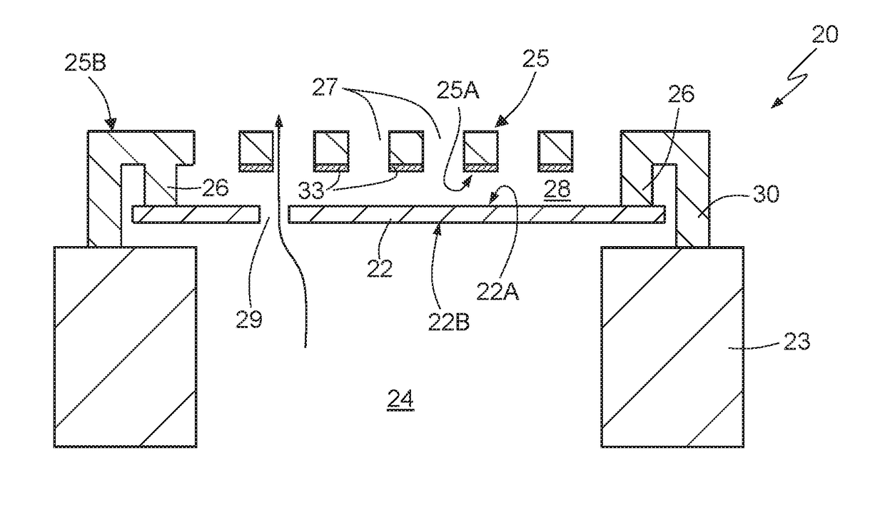
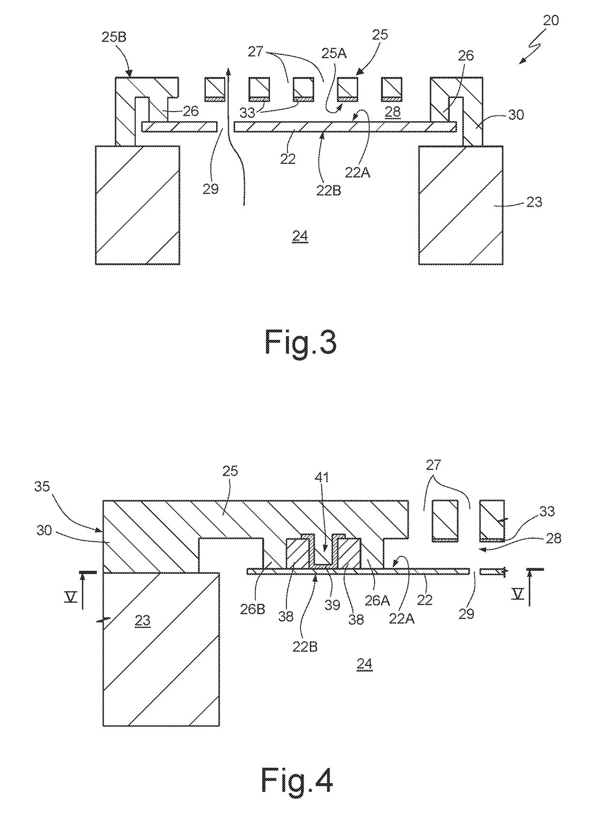
[0022]FIG. 3 schematically shows the structure of the present transducer, designated as a whole by 20.

[0023]The transducer 20 is of a fully clamped back plate type and comprises a substrate 23 of semiconductor material such as silicon, housing a cavity 24, of a through hole type, and carrying a back plate 25 through a plate anchor region 30. The back plate 25, of insulating material, such as silicon nitride, has a first surface 25A facing the substrate 23, and a second surface 25B, facing in the opposite direction. A fixed electrode 33 of conductive material, for example doped polycrystalline silicon, extends over the first surface 25A. A membrane 22 of conductive material, for example doped polycrystalline silicon, faces the fixed electrode 33 and is carried by the back plate 25 through a membrane anchoring structure 26. The membrane anchoring structure 26, of insulating material, for example of the same material as the back plate 25 and formed simultaneously and monolithically the...


PUM

PropertyMeasurementUnit
frequencyaaaaaaaaaa
frequencyaaaaaaaaaa
thicknessaaaaaaaaaa

Abstract

An electroacoustic MEMS transducer, having a substrate of semiconductor material; a through cavity in the substrate; a back plate carried by the substrate through a plate anchoring structure, the back plate having a surface facing the through cavity; a fixed electrode, extending over the surface of the back plate; a membrane of conductive material, having a central portion facing the fixed electrode and a peripheral portion fixed to the surface of the back plate through a membrane anchoring structure; and a chamber between the membrane and the back plate, peripherally delimited by the membrane anchoring structure.

Description

BACKGROUNDTechnical Field[0001]The present disclosure relates to an integrated electroacoustic transducer of a MEMS (Micro-Electro-Mechanical System) type with improved sensitivity, and to the manufacturing process thereof.Description of the Related Art[0002]As is known, MEMS techniques of micromachining semiconductor devices enable production of micrometric structures within layers of semiconductor material, deposited (for example, polycrystalline silicon layers) or grown (for example, epitaxial layers) over sacrificial layers and / or other semiconductor or insulating layers, which are at least partially removed through chemical etching to form mobile or flexible regions.[0003]In particular, MEMS electroacoustic transducers are known, comprising a flexible membrane integrated in or on a semiconductor die. FIGS. 1A and 1B represents schematically, by way of example, a transducer 1 of the back plate and semi-clamped type.[0004]The transducer 1 comprises a membrane 2 carried by a subst...

Claims


Application Information

Patent Timeline
Patent Type & Authority Applications(United States)
IPC IPC(8): H04R7/18B81B3/00B81C1/00H04R19/04H04R19/00
CPCH04R7/18B81B3/0054B81C1/00158H04R19/04B81B2203/0127B81B2203/0307B81B2201/0257B81B2203/0315B81C2201/0132H04R19/005B81B3/0072
Inventor PERLETTI, MATTEOLOSA, STEFANOTENTORI, LORENZOTURI, MARIA CAROLINA
Owner STMICROELECTRONICS SRL
Why Eureka
Try Eureka