NETWORK PROCESSOR FPGA (npFPGA): MULTI-DIE-FPGA CHIP FOR SCALABLE MULTI-GIGABIT NETWORK PROCESSING

a network processing and chip technology, applied in the field of multi-die integrated circuit devices, can solve the problems of multiple fpga chips, inability to scale to the desired port density, aggregation, wire speed throughput, etc., and achieve the effect of reducing power consumption of multi-die devices

Active Publication Date: 2018-06-14
ALTERA CORP
View PDF2 Cites 6 Cited by
  • Summary
  • Abstract
  • Description
  • Claims
  • Application Information

AI Technical Summary

Benefits of technology

[0005]In light of the above, the present disclosure relates to a multi-die device, such as a network processor FPGA (npFPGA), having FPGA dies and at least one network interface controller (NIC) die, and systems and methods for reducing power consumption of such a multi-die device. A multi-die device of the present disclosure allows implementation of scalable and user-definable network processing functions at wire speed, comparable to ASSP and ASIC devices. A multi-die device of the present disclosure may be targeted for a wide range of applications, similar to a hardwired ASIC or ASSP / network processor devices.
[0006]An npFPGA of the present disclosure may offer a significant advantage compared to traditional network processing hardware solutions in terms of scalability, system architecture flexibility, customization, and product differentiation. Compared to ASICs, an npFPGA may have a lower development cost and faster development cycle. Compared to ASSPs or network processors, an npFPGA allows more system architecture flexibility. Customers may easily integrate proprietary hardware and software to customize an npFPGA with a high degree of product differentiation, and an npFPGA may be easily upgraded. Compared to using multiple FPGA chips, an npFPGA may offer higher performance with low area utilization, offering high port density.
[0008]In accordance with additional embodiments of the present disclosure, there is provided a method for reducing power consumption of a multi-die device, such as an npFPGA. Usage of hardware resources (e.g., FPGA dies, NIC dies, memory dies, or processing elements implemented within the FPGA fabric) in the multi-die device may be monitored. One of the hardware resources that is not in use may be identified, and control circuitry may be used to gate power to the identified hardware resource.
[0009]In accordance with additional embodiments of the present disclosure, there is provided a system for reducing power consumption of a multi-die device having multiple processing elements (PEs) implemented within the FPGA fabric. A function scheduler associated with a group of the PEs may monitor task requests from a task queue, assign a task from the task queue to one of the PEs in the group, monitor progress of the assigned task, and post a result in an output descriptor queue when the assigned task has been completed. The function scheduler may gate power to unused PEs in the group.

Problems solved by technology

ASIC, ASSP, and network processor devices may be costly to develop or difficult to upgrade.
Current FPGA implementations (e.g., use of multiple FPGA chips) may not offer or scale to the desired port density, aggregation, or wire speed throughput.

Method used


Image

  • NETWORK PROCESSOR FPGA (npFPGA): MULTI-DIE-FPGA CHIP FOR SCALABLE MULTI-GIGABIT NETWORK PROCESSING
  • NETWORK PROCESSOR FPGA (npFPGA): MULTI-DIE-FPGA CHIP FOR SCALABLE MULTI-GIGABIT NETWORK PROCESSING
  • NETWORK PROCESSOR FPGA (npFPGA): MULTI-DIE-FPGA CHIP FOR SCALABLE MULTI-GIGABIT NETWORK PROCESSING

Examples


Embodiment Construction

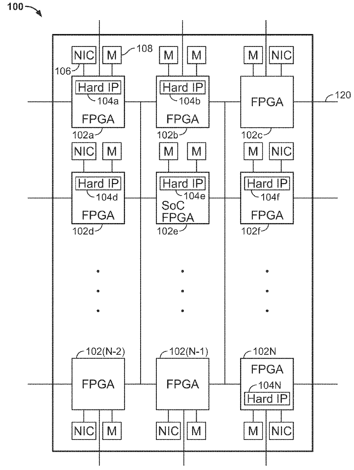
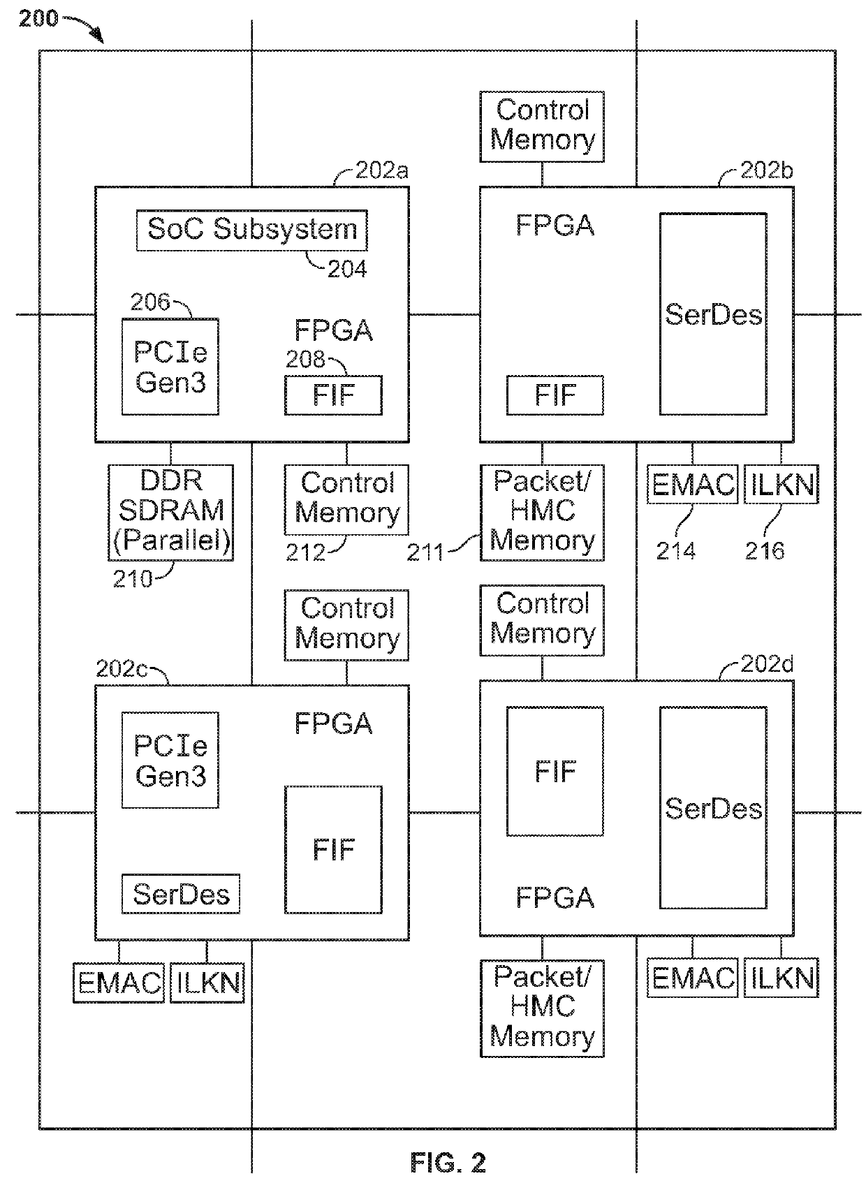
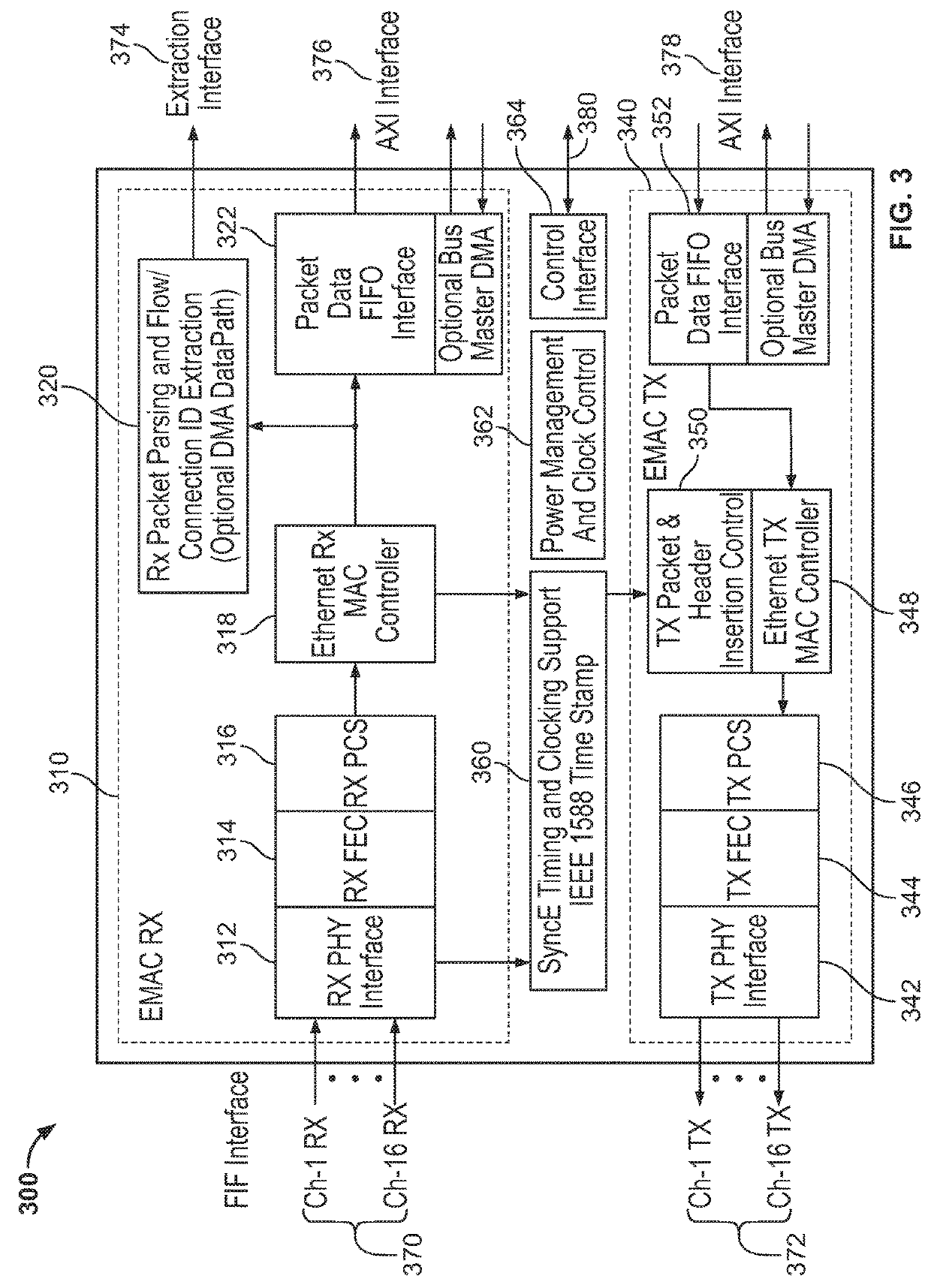
[0023]To provide an overall understanding of the invention, certain illustrative embodiments will now be described. However, it will be understood by one of ordinary skill in the art that the systems and methods described herein may be adapted and modified as is appropriate for the application being addressed and that the systems and methods described herein may be employed in other suitable applications, and that such other additions and modifications will not depart from the scope hereof.

[0024]The figures described herein show illustrative embodiments; however, the figures may not necessarily not show and may not be intended to show the exact layout of the hardware components contained in the embodiments. The figures are provided merely to illustrate the high-level conceptual layouts of the embodiments. The embodiments disclosed herein may be implemented with any suitable number of components and any suitable layout of components in accordance with principles known in the art.

[002...


PUM


Abstract

Systems and methods are provided for reducing power consumption of a multi-die device, such as a network processor FPGA (npFPGA). The multi-die device may include hardware resources such as FPGA dies, which may be coupled to NIC dies and / or memory dies. Power consumption of the multi-die device may be reduced by monitoring usage of hardware resources in the multi-die device, identifying hardware resources that are not in use, and gating power to the identified hardware resources. The status of processing elements (PEs) in the multi-die device may be tracked in a PE state table. Based on the PE state table, tasks from a task queue may be assigned to one or more processing elements.

Description

CROSS-REFERENCE[0001]This is a continuation, and claims the benefit of U.S. application Ser. No. 13 / 921,364, filed Jun. 19, 2013, the contents of which are incorporated by reference in their entirety.FIELD OF THE DISCLOSURE[0002]This disclosure relates to multi-die integrated circuit devices, such as field programmable gate array (FPGA) devices, and systems and methods for reducing power consumption of such devices.BACKGROUND OF THE DISCLOSURE[0003]Ethernet has become a widely used connectivity solution because of its scalability; speeds may range from sub-gigabit to multi-gigabit. Ethernet may be used for work stations, local area networks (LANs), wide area networks (WANs), metropolitan area networks (MANs), the Internet backbone, and data centers to perform computing, storage, and networking functions. Ethernet networking systems may vary in the nature of packet processing and traffic management functions depending on the application and standard requirements.[0004]Packet processi...

Claims


Application Information

Patent Timeline
Patent Type & Authority Applications(United States)
IPC IPC(8): G06F1/32
CPCG06F1/32G06F1/329Y02D10/00
Inventor VENKATARAMAN, KRISHNAN
Owner ALTERA CORP
Why Eureka
Try Eureka