Physical design in magnetic environment

a physical design and magnetic environment technology, applied in the direction of transformers/inductance coils/windings/connections, inductances, and semiconductor/solid-state device details, can solve the problems of affecting the overall system performance, and affecting the shielding of on-chip circuitry from magnetic fields

Active Publication Date: 2018-07-05
SILICON LAB INC
View PDF3 Cites 4 Cited by
  • Summary
  • Abstract
  • Description
  • Claims
  • Application Information

AI Technical Summary

Problems solved by technology

However, in other applications, (e.g., oscillator applications) this coupling is undesirable since it may induce unwanted voltages and / or currents within neighboring circuitry.
That unwanted coupling can degrade overall system performance.
Shielding on-chip circuitry from magnetic fields can be challenging when magnetic materials are not available.

Method used


Image

  • Physical design in magnetic environment
  • Physical design in magnetic environment
  • Physical design in magnetic environment

Examples


Embodiment Construction

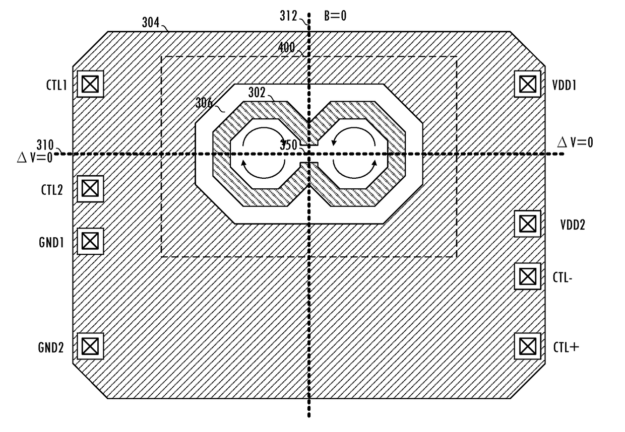
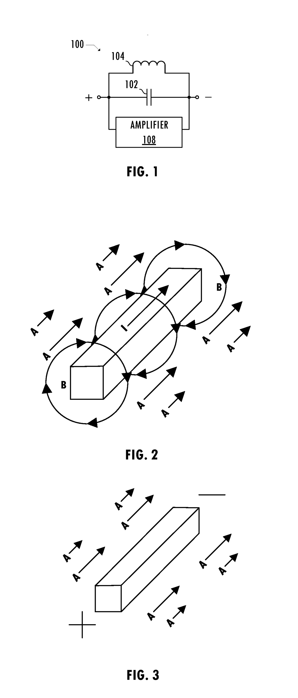
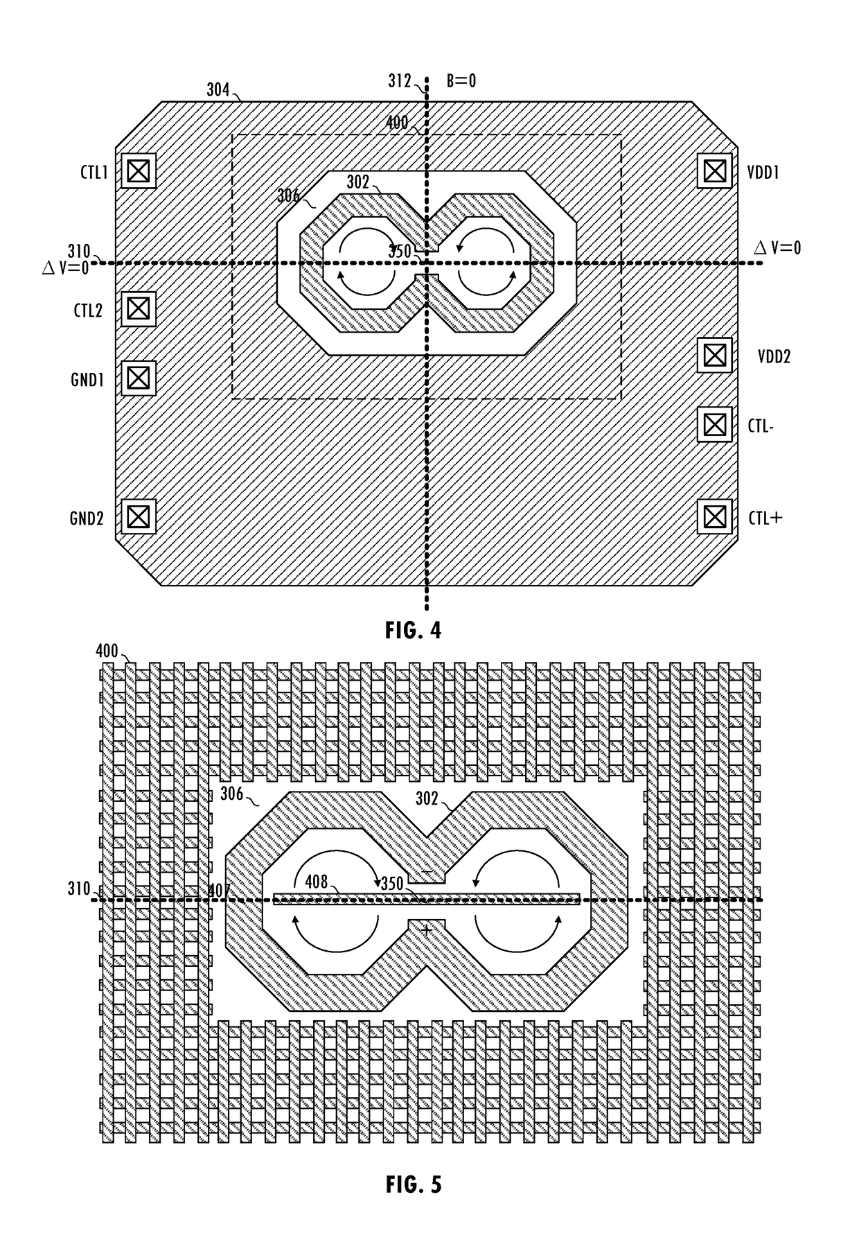
[0004]In at least one embodiment, an integrated circuit includes an inductor having a first axis through a center of the inductor and a second axis through the center of the inductor. The first axis is a first nodal axis and includes a first location of a first magnetic node having a first negligible induced voltage amplitude at a distance from the center of the inductor. The second axis is a first anti-nodal axis and includes a second location of a first negligible magnetic flux density field and a first induced voltage amplitude greater than the first negligible induced voltage amplitude at the distance from the center of the inductor. The integrated circuit includes a first cluster of integrated circuit terminals concentrated about the first axis and distant from the second axis. The first negligible induced voltage amplitude may be a minimum induced voltage amplitude at the distance from the center of the inductor and the first induced voltage amplitude may be a maximum induced ...


PUM

PropertyMeasurementUnit
magnetic flux densityaaaaaaaaaa
induced voltage amplitudeaaaaaaaaaa
electrically conductiveaaaaaaaaaa

Abstract

A technique for forming an integrated circuit including an inductor reduces magnetic coupling between the inductor and surrounding elements. The technique includes deliberate placement of circuit elements (e.g., terminals, pins, routing traces) in locations on the integrated circuit relative to a magnetic vector potential associated with the inductor and relative to a magnetic flux density field associated with the inductor to reduce or eliminate induced signals that degrade system performance.

Description

BACKGROUNDField of the Invention[0001]The present application relates to integrated circuits, and more particularly to integrated circuits that include inductor structures.Description of the Related Art[0002]In general, electronic oscillator circuits are used to generate repetitive oscillating electronic signals for a variety of integrated circuit applications (e.g., local oscillator signals for radio frequency mixers, transmitters for generating carrier waves for radio frequency signal transmission, etc.). Referring to FIG. 1, a clock generator circuit may use conventional tank circuit 100, which is a tuned circuit including inductor 104 coupled to capacitor 102. Charge flows back and forth from the plates of capacitor 102 through the inductor so the tuned circuit can store electrical energy oscillating at its resonant frequency. Amplifier circuit 108 compensates for small losses in conventional tank circuit 100 to sustain oscillation. By supplying a transconductance that is equal ...

Claims


Application Information

Patent Timeline
Patent Type & Authority Applications(United States)
IPC IPC(8): H01F27/34H01F27/28H01F41/04H01F27/36H01L23/50H01L49/02H01L23/552H01L23/58
CPCH01F27/34H01F27/2804H01F41/041H01L23/585H01L23/50H01L28/10H01L23/552H01F27/365H01L21/707H01L27/016H01F27/363H01F17/0006H01F2017/0073H01L23/645H01L23/66H01F27/36
Inventor CAFFEE, AARON J.DROST, BRIAN G.
Owner SILICON LAB INC
Why Eureka
Try Eureka