Antenna-integrated type communication module and manufacturing method for the same

a communication module and integrated technology, applied in the structure of radiating elements, individual energised antenna arrays, particular array feeding systems, etc., can solve the problems of difficult to maintain a high communication speed and large transmission loss, and achieve the effect of increasing the number of radiation elements, high communication speed, and ensuring the characteristics of adaptive array antennas

Active Publication Date: 2018-07-19
MURATA MFG CO LTD
View PDF3 Cites 32 Cited by
  • Summary
  • Abstract
  • Description
  • Claims
  • Application Information

AI Technical Summary

Benefits of technology

[0008]A high communication speed can be achieved by using an adaptive array antenna including a large number of radiation elements. With a communication scheme using an adaptive array antenna, by controlling a phase and amplitude of each input-output signal of the large number of radiation elements, a transmission / reception path can be optimized by incorporating reflection from the ceiling, furniture, or the like. Of the adaptive array antennas, an antenna configured to control only a phase of each input-output signal of a large number of radiation elements is called a phased array antenna. The phased array antenna is widely used because the configuration thereof is simpler than that of the adaptive array antenna configured to control both a phase and amplitude.
[0036]Because bar-shaped conductors to become the feeding wires are connected to the lands disposed on the upper surface of the multilayer substrate, a wiring pattern can be disposed inside the multilayer substrate without the wiring pattern being separated from the positions of the conductor pins, lands, and the like. In addition, when a transmission / reception circuit component is mounted on the bottom surface of the multilayer substrate, it is unnecessary for the circuit component to be separate from the positions of the conductor pins. Because the second dielectric layer is so formed on the multilayer substrate as to cover the conductor pins, it is possible to enhance the bonding strength between the multilayer substrate and the second dielectric layer in comparison with a case in which a dielectric substrate corresponding to the second dielectric layer is bonded to the multilayer substrate by soldering, or the like.

Problems solved by technology

However, in the case of the millimeter waveband, the transmission loss becomes large because of the radio waves being reflected and absorbed by a shielding object such as a human body, furniture, or the like.
Such large transmission loss makes it difficult to maintain a high communication speed.

Method used


Image

  • Antenna-integrated type communication module and manufacturing method for the same
  • Antenna-integrated type communication module and manufacturing method for the same
  • Antenna-integrated type communication module and manufacturing method for the same

Examples


first embodiment

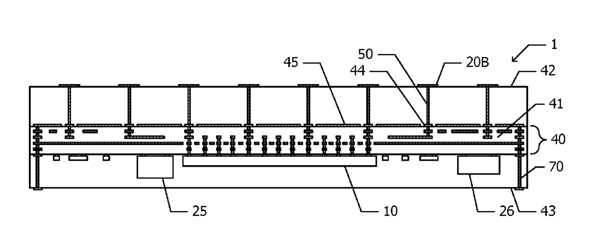
[0049]FIG. 1 illustrates a block diagram of an antenna-integrated type communication module 1 according to a first embodiment. The antenna-integrated type communication module 1 according to the first embodiment includes a phased array antenna of 32 elements configured to control only a phase, and is used in communications using millimeter waves of the 60 GHz band.

[0050]Radiation elements 20 of 32 pieces are each connected to an input-output terminal 11 of a transmission / reception circuit component 10. Each of the input-output terminals 11 is selectively connected to one of a reception low noise amplifier 13 and a transmission power amplifier 14 via a switch (transmission / reception switching device) 12. The radiation element 20 is normally connected to the reception low noise amplifier 13, and is connected to the transmission power amplifier 14 only at the time of transmission.

[0051]An output of the reception low noise amplifier 13 is inputted to a phase shifter 15 for reception. Ou...

second embodiment

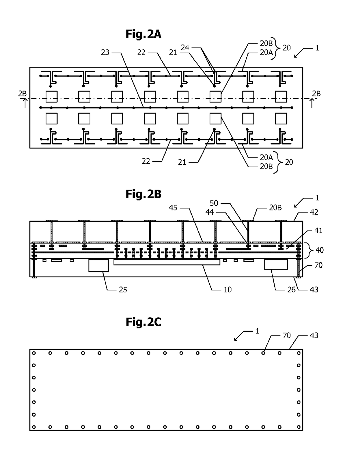
[0095]Next, the antenna-integrated type communication module 1 according to a second embodiment will be described with reference to FIG. 8A and FIG. 8B. Hereinafter, different points from the first embodiment will be described, and description of the same constituent elements will be omitted.

[0096]FIG. 8A and FIG. 8B respectively illustrate a cross-sectional view and a bottom view of the antenna-integrated type communication module 1 according to the second embodiment. In the second embodiment, the upper surface of the second dielectric layer 42 includes a flat region 46 parallel to the upper surface of the multilayer substrate 40, and a slant region 47 being slanted relative to the flat region 46. The slant region 47 is continuously connected to the flat region 46 at both ends of the flat region 46. The slant region 47 is slanted in such a direction that a normal direction 46n of the flat region 46 and a normal direction 47n of the slant region 47 are distanced from each other as t...


PUM


Abstract

A multilayer substrate includes a first dielectric layer and a conductor pattern disposed in at least an interior of the first dielectric layer. A second dielectric layer formed of a different material from a material of the first dielectric layer is disposed on the multilayer substrate. At least one radiation element is formed on the second dielectric layer. A feeding wire connects the radiation element and the conductor pattern. The feeding wire includes a conductor pin that is conductive and extends in a thickness direction of the second dielectric layer. The conductor pin electrically connects the radiation element and the conductor pattern. Provided is an antenna-integrated type communication module having such a structure that the accuracy of circuit simulation is easily enhanced and the degree of freedom in selection of dielectric materials is large.

Description

[0001]This is a continuation of International Application No. PCT / JP2016 / 075695 filed on Sep. 1, 2016 which claims priority from Japanese Patent Application No. 2015-183533 filed on Sep. 17, 2015. The contents of these applications are incorporated herein by reference in their entireties.BACKGROUND OF THE DISCLOSUREField of the Disclosure[0002]The present disclosure relates to an antenna-integrated type communication module and its manufacturing method.Description of the Related Art[0003]An antenna-integrated type communication module in which a high frequency circuit module (a transmission / reception circuit component) and an antenna element (a patch antenna) are integrated is disclosed in Patent Document 1 cited below. In the disclosed antenna-integrated type communication module, a first conductor layer, a first dielectric layer, a second conductor layer, a second dielectric layer, and a third conductor layer are laminated in that order from above.[0004]The patch antenna is dispos...

Claims


Application Information

Patent Timeline
Patent Type & Authority Applications(United States)
IPC IPC(8): H01Q21/00H01Q1/38H01Q3/26H01Q1/22H01Q21/06H01L23/66
CPCH01Q21/0025H01Q1/38H01Q3/2605H01Q21/0087H01Q1/2291H01Q21/065H01L23/66H01L2223/6677H01Q3/26H01Q23/00H01L2224/16227H01L2924/15159H01L2924/1532H01L2924/1533H01Q21/062H01Q21/067H01Q25/00H04B7/00
Inventor MIZUNUMA, RYUKENBANBA, SHINICHIROYOKOYAMA, MICHIHARUUEDA, HIDEKIYAMADA, HIDEAKIMORIOKA, NOBORU
Owner MURATA MFG CO LTD
Why Eureka
Try Eureka