Electron channeling pattern acquisition from small crystalline areas

a technology of electron channeling pattern and crystalline material, which is applied in the field of crystal analysis, can solve the problems of affecting device performance and generating crystalline defects, and achieve the effect of accurate identification of crystal structure and orientation, and increased effective angular rang

Active Publication Date: 2018-07-26
IBM CORP
View PDF0 Cites 2 Cited by
  • Summary
  • Abstract
  • Description
  • Claims
  • Application Information

AI Technical Summary

Benefits of technology

[0004]In accordance with an embodiment of the present invention, a method for crystal analysis includes identifying a crystalline region on a device where an electronic channeling pattern is needed to determine the exact crystal orientation of the crystalline area with respect to the electron beam. A partial image of the whole electron channeling pattern (ECP) is acquired for each of a number of different positions of the crystalline region with respect to the electron beam using a scanning electron microscope (SEM). After a partial image of the ECP is acquired, the position of the crystalline region is translated using the SEM stage to physically move the crystalline region to an at least one new location in the SEM microscope and an at least second image is taken with the SEM. The partial images of the ECP are stitched together to form a composite map of a larger portion of the ECP. This larger area of the ECP provides an increase in effective angular range between a SEM beam and a surface of the crystalline region allowing for more accurate identification of crystal structure and orientation.

Problems solved by technology

Such techniques can be prone to crystalline defect generation which can have deleterious effects on device performance.
Crystalline defects are most often not visible to conventional non-destructive techniques such as conventional scanning electron microscopy (SEM) and optical tools.
However, for manufacturing control, the statistics of the distribution of defects from a much larger area is required because defects are known to affect performance and reliability adversely.

Method used


Image

  • Electron channeling pattern acquisition from small crystalline areas
  • Electron channeling pattern acquisition from small crystalline areas
  • Electron channeling pattern acquisition from small crystalline areas

Examples


Embodiment Construction

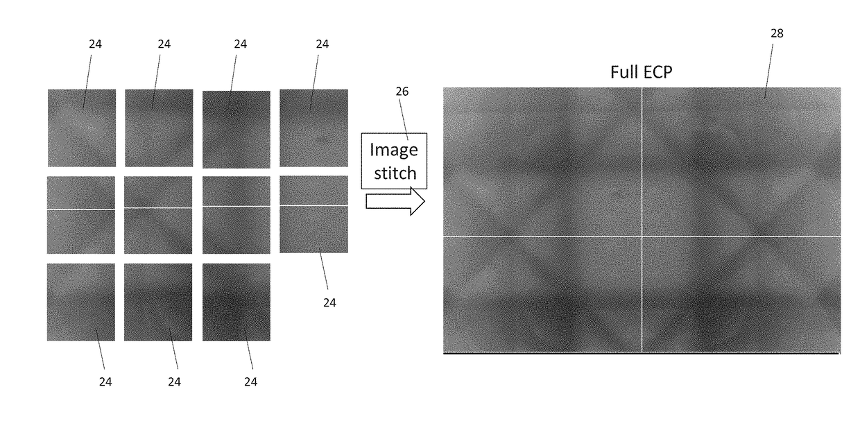
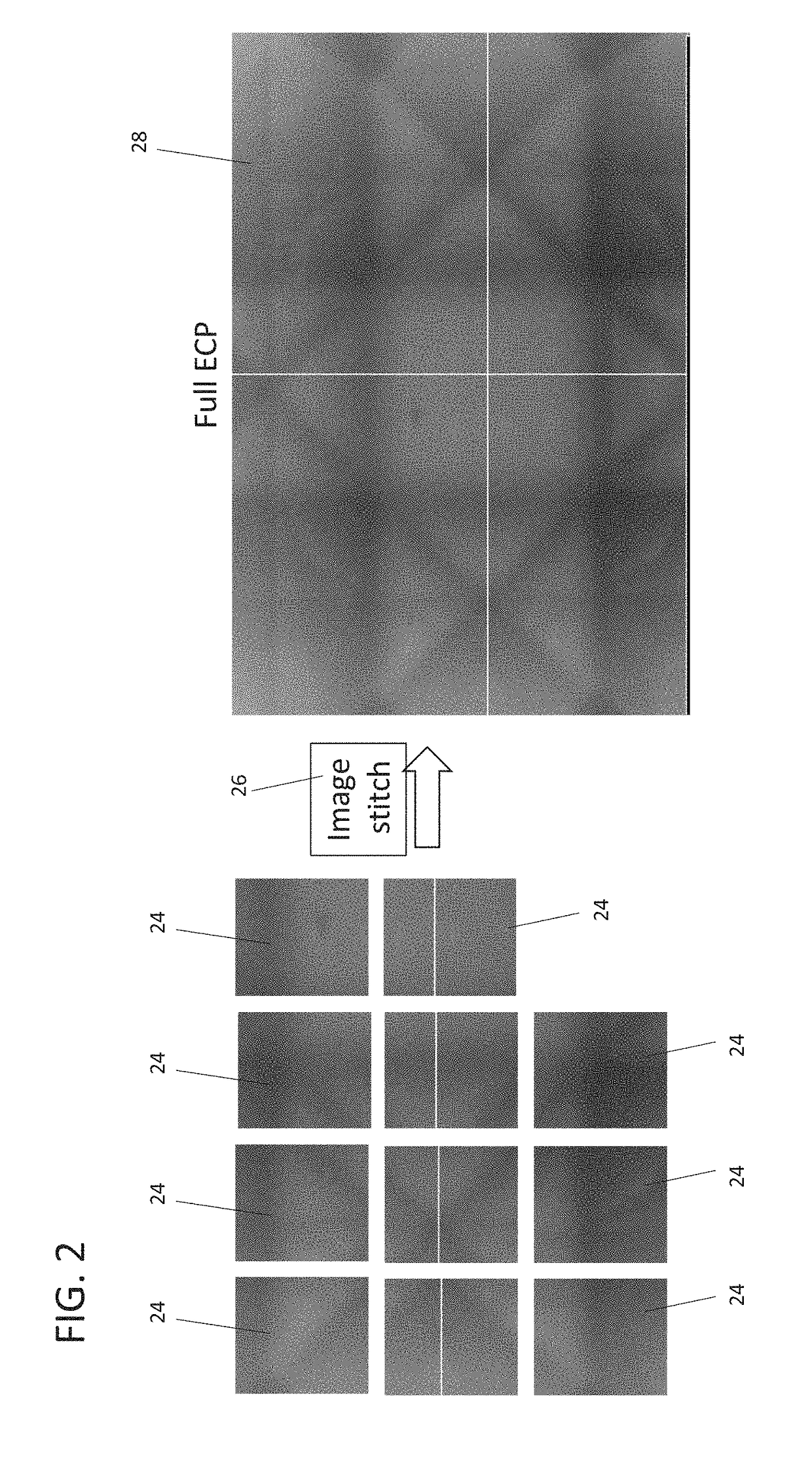
[0018]In accordance with embodiments of the present invention, systems and methods are provided for determining electron channel patterns on samples with only small areas of crystalline material. In particularly useful embodiments, electronic channel patterns are employed to determine exact alignment of the crystalline material and the electron beam in an SEM to acquire electron channeling contrast images (ECCI) which help to map and detect defects in crystal / crystalline materials. To determine crystal structure and orientation, a plurality of images of partial ECP images are stitched together to create a complete map or full ECP for a substrate, chip or device.

[0019]In accordance with one embodiment, ECCI is employed as a technique for rapid and high resolution characterization of individual crystalline defects in a scanning electron microscope (SEM). However, in accordance with the present embodiments, the ECCI application is no longer limited to bare semiconductor material sample...


PUM


Abstract

A method for crystal analysis includes identifying a crystalline region on a device where an electronic channeling pattern is needed to be determined, acquiring a whole image for each of a plurality of different positions for the crystalline region using a scanning electron microscope (SEM) as the crystalline region is moved to different positions. Relevant regions are extracted from the whole images. The images of the relevant regions are stitched together to form a composite map of a full electron channeling pattern representative of the crystalline region wherein the electronic channeling pattern is provided due to an increase in effective angular range between a SEM beam and a surface of the crystal region.

Description

BACKGROUNDTechnical Field[0001]The present invention generally relates to crystal analysis, and more particularly to systems and methods for acquiring images for identifying an electron channeling pattern in a crystalline material.Description of the Related Art[0002]Continued performance improvements in devices require heterogeneous integration of different materials, nanoscale fin geometry, as well as synthesis of metastable phases. Such techniques can be prone to crystalline defect generation which can have deleterious effects on device performance. Crystalline defects are most often not visible to conventional non-destructive techniques such as conventional scanning electron microscopy (SEM) and optical tools.[0003]Methods for improving transistor performance include the introduction of permanent strain in a channel region using either external stressor or strained epitaxial channel layers. Along with the introduction of strain in complementary metal oxide semiconductor (CMOS) te...

Claims


Application Information

Patent Timeline
Patent Type & Authority Applications(United States)
IPC IPC(8): G06T7/00H01J37/22G06K9/46G06T11/60H01J37/29
CPCG06T2207/30148G06T2207/10056H01J37/222G06T7/0004G06K9/4604G06T11/60H01J37/292G06T2200/32G06T2207/10016G06T2207/10061G06T7/33G06V20/693
Inventor BEDELL, STEPHEN W.MUKHERJEE, KUNALOTT, JOHN A.SADANA, DEVENDRA K.WACASER, BRENT A.
Owner IBM CORP
Why Eureka
Try Eureka