GLASS WAVEGUIDE ASSEMBLIES FOR OE-PCBs AND METHODS OF FORMING OE-PCBs

a technology of optical waveguides and optical waveguides, applied in the direction of optical elements, printed circuit non-printed electric components association, instruments, etc., can solve the problems of relatively low yield, manufacturing complexity, manufacturing inefficiencies, etc., and achieve the effect of simplifying the oe-pcb fabrication process and increasing throughpu

Active Publication Date: 2018-08-02
CORNING OPTICAL COMM LLC
View PDF1 Cites 11 Cited by
  • Summary
  • Abstract
  • Description
  • Claims
  • Application Information

AI Technical Summary

Benefits of technology

The patent text describes a new way to make printed circuit boards (PCBs) that have added optical, mechanical, and / or electrical features. The process uses a glass sheet that has these features added to it before it is made into a PCB. This makes it compatible with standard PCB steps like lamination, drilling, and plating. The glass sheet can be processed like other flexible sheets used for PCBs. The glass waveguide assembly is made of a thin sheet of glass with optical waveguides added to it. The assembly can be combined with other PCB processes to make the final PCB. A protective coating can be added to the glass waveguide assembly to make it easier to process, and one or more of the assemblies can be combined with other PCB processes to make the final PCB.

Problems solved by technology

To date this has proven to be relatively complex and costly due in large measure to the glass substrates not being sufficiently compatible with standard PCB fabrication and assembly techniques.
This has resulted in manufacturing inefficiencies, fabrication complexity, relatively low yield and high cost for OE-PCBs.

Method used


Image

  • GLASS WAVEGUIDE ASSEMBLIES FOR OE-PCBs AND METHODS OF FORMING OE-PCBs
  • GLASS WAVEGUIDE ASSEMBLIES FOR OE-PCBs AND METHODS OF FORMING OE-PCBs
  • GLASS WAVEGUIDE ASSEMBLIES FOR OE-PCBs AND METHODS OF FORMING OE-PCBs

Examples


Embodiment Construction

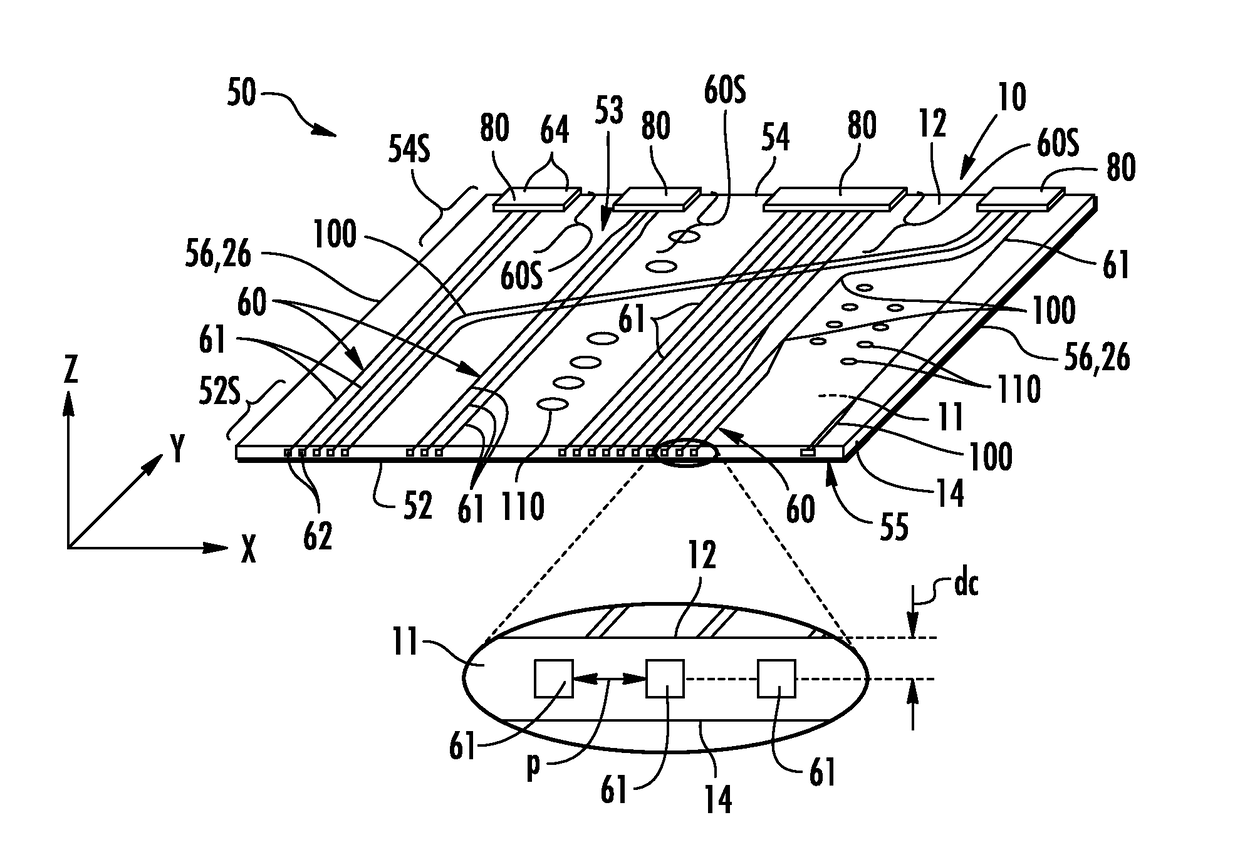
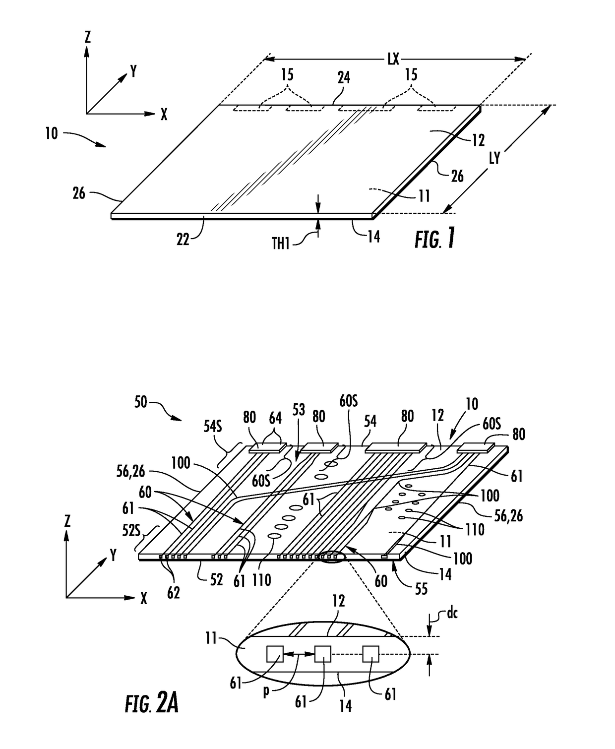
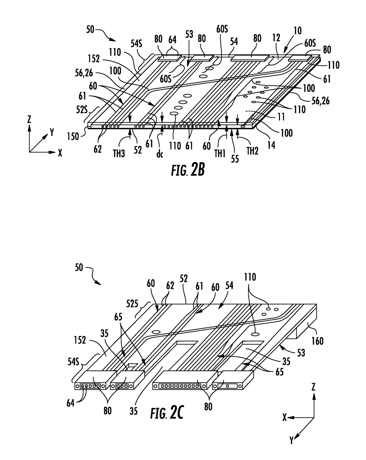
[0035]Reference is now made in detail to various embodiments of the disclosure, examples of which are illustrated in the accompanying drawings. Whenever possible, the same or like reference numbers and symbols are used throughout the drawings to refer to the same or like parts. The drawings are not necessarily to scale, and one skilled in the art will recognize where the drawings have been simplified to illustrate the key aspects of the disclosure.

[0036]The claims as set forth below are incorporated into and constitute part of this Detailed Description.

[0037]Cartesian coordinates are shown in some of the Figures for the sake of reference and are not intended to be limiting as to direction or orientation.

[0038]The acronym “MT” means “mechanical transfer” and is used to describe a type of multi-fiber optical fiber connector, in which two mechanical pins dictate the alignment of the optical fibers, or in the present disclosure a multi-waveguide connector. The typical outer dimensions o...


PUM


Abstract

The glass waveguide assembly includes a substrate with glass optical waveguides formed in the body of the glass substrate without adding or removing any glass from the substrate body. The glass optical waveguides run generally from a front-end section to a back-end section. A protective coating is formed over at least a portion of the top surface of the glass substrate where the glass optical waveguides reside. Optical connectors are formed at or adjacent the back end at corresponding connector regions. Each connector includes an end portion of at least one of the glass optical waveguides. In some configurations, the glass waveguide assembly includes a bend section that facilitates forming an optical interconnection in a photonic system between an optical-electrical printed circuit board and photonic integrated circuit.

Description

FIELD[0001]The present disclosure relates to optical-electrical printed circuit boards (OE-PCBs), and in particular relates to glass waveguide assemblies for OE-PCBs and methods of forming OE-PCBs.BACKGROUND[0002]Photonic systems are based on the generation, manipulation and / or detection of light much in the way electronic systems are based on generation, manipulation and / or detection of electricity. Photonic systems can also be based on the generation, manipulation and / or detection of both light and electricity, in which case they are sometimes referred to as opto-electronic systems.[0003]A key component of photonic systems is an OE-PCB. The OE-PCB typically includes optical waveguides to conduct light much in the way conventional electrical-based PCBs use wiring to conduct electricity. The OE-PCB also includes electrical wires and components usually associated with conventional electrical-based PCBs. The OE-PCB can also include optical components such light emitters, light detecto...

Claims


Application Information

Patent Timeline
Patent Type & Authority Applications(United States)
IPC IPC(8): G02B6/122G02B6/30G02B6/134G02B6/42
CPCG02B6/122G02B6/30G02B2006/12102G02B6/428G02B6/1345G02B6/4204G02B6/4214G02B6/4249G02B6/43H05K1/0274H05K1/18H05K1/189G02B2006/12038G02B2006/12183H05K2201/053H05K2201/10446
Inventor BRUSBERG, LARS MARTIN OTFRIED
Owner CORNING OPTICAL COMM LLC
Why Eureka
Try Eureka