Semiconductor chip

a technology of semiconductors and semiconductors, applied in the field of semiconductors, can solve the problems of reducing the mounting area, affecting the characteristics of the transistor, and increasing the temperature, so as to reduce the mounting area and restrain the influence of the heat generated by the transistor

Active Publication Date: 2018-08-02
MURATA MFG CO LTD
View PDF1 Cites 9 Cited by
  • Summary
  • Abstract
  • Description
  • Claims
  • Application Information

AI Technical Summary

Benefits of technology

[0005]The present disclosure has been made in view of the circumstances described above, and it is an object of the disclosure to provide a semiconductor chip that can reduce the influences exerted by the heat generated by a transistor while providing a reduced mounting area.
[0007]According to the present disclosure, a semiconductor chip is provided that can reduce a mounting area and also restrain the influences of the heat generated by a transistor.

Problems solved by technology

Therefore, when the transistor generates heat due to its amplifying operation, an increase in temperature may change the characteristics of the transistor.
Using the foregoing flip chip technology for such a power amplifier circuit will pose a problem in that heat will not be adequately dissipated, affecting the characteristics of the transistor, although the mounting area will be reduced.

Method used


Image

  • Semiconductor chip
  • Semiconductor chip
  • Semiconductor chip

Examples


second embodiment

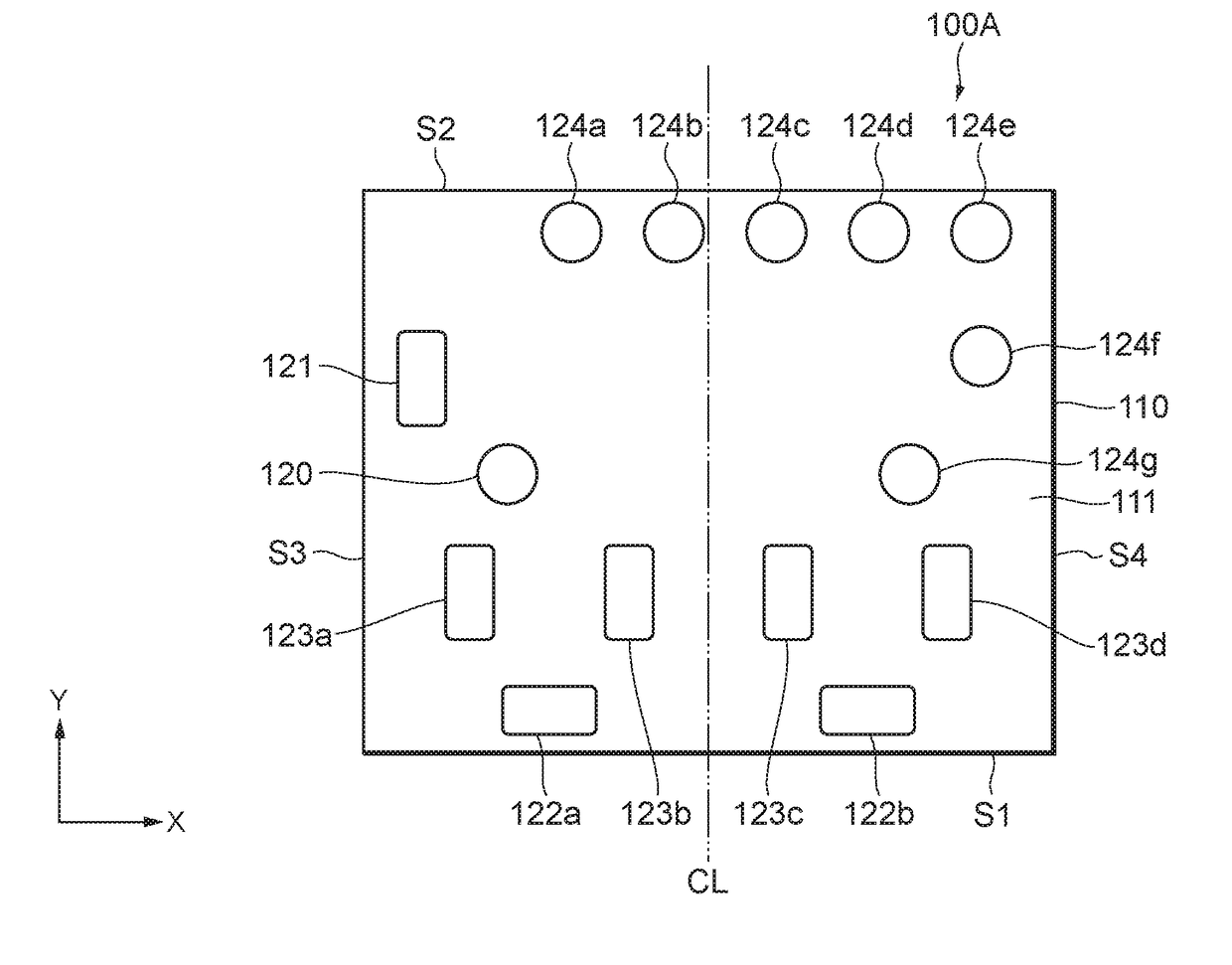
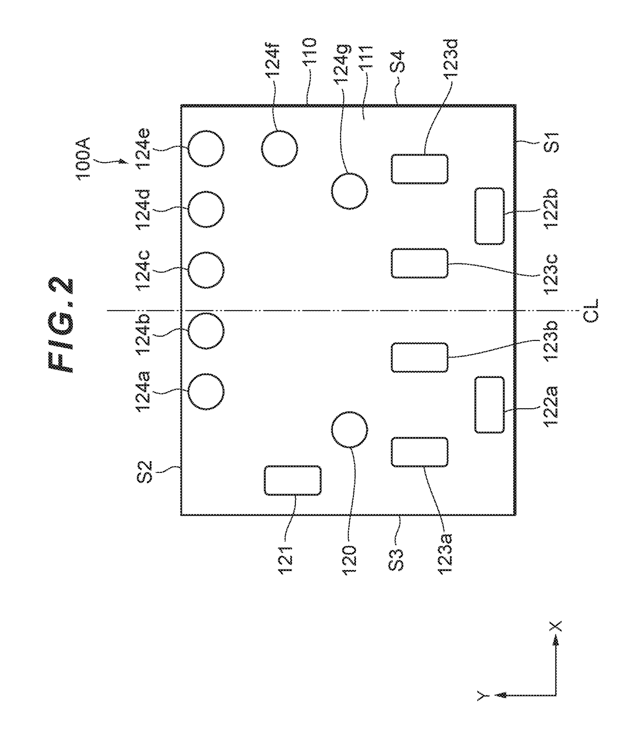
[0035]FIG. 3 is a plan view of a semiconductor chip according to the present disclosure. A semiconductor chip 100B illustrated in FIG. 3 differs from the semiconductor chip 100A illustrated in FIG. 2 in the shapes of bumps connected to the collector of a transistor Q2. More specifically, the semiconductor chip 100B includes bumps 222a and 222b in place of the bumps 122a and 122b.

[0036]As with the bumps 122a and 122b, the bumps 222a (a first part of a third bump) and 222b (a second part of the third bump) are connected to the collector of the transistor Q2, and outputs an amplified signal RF3, which is output from the transistor Q2, to an element outside the semiconductor chip 100B. Further, each of the bumps 222a and 222b is disposed such that the long side direction in the vicinity of a side S1 is substantially parallel to an X-axis. A length L2 of the long side direction (the X-axis direction in FIG. 3) of each of the bumps 222a and 222b is greater than a length L1 of the long si...

third embodiment

[0037]FIG. 4 is a plan view of a semiconductor chip according to the present disclosure. A semiconductor chip 100C illustrated in FIG. 4 differs from the semiconductor chip 100A illustrated in FIG. 2 in the shapes of bumps connected to the collector of a transistor Q2. More specifically, the semiconductor chip 100C includes bumps 322a and 322b in place of the bumps 122a and 122b.

[0038]As with the bumps 122a and 122b, the bumps 322a (a first part of a third bump) and 322b (a second part of the third bump) are connected to the collector of the transistor Q2, and outputs an amplified signal RF3, which is output from the transistor Q2, to an element outside the semiconductor chip 100C. Further, each of the bumps 322a and 322b is disposed such that the long side direction in the vicinity of a side S1 is substantially parallel to an X-axis. A length L3 of the long side direction (the X-axis direction in FIG. 3) of each of the bumps 322a and 322b is smaller than a length L1 of the long si...

fourth embodiment

[0042]FIG. 5 is a plan view of a semiconductor chip according to the present disclosure. A semiconductor chip 100D illustrated in FIG. 5 includes an additional bump 400, as compared with the semiconductor chip 100C illustrated in FIG. 4.

[0043]The bump 400 (a sixth bump) is electrically connected to a part of a harmonic termination circuit, which is a specific example of a filter circuit which attenuates a harmonic (e.g. a second harmonic, a third harmonic, or a fourth harmonic) of an amplified signal RF3 output from the collector of a transistor Q2. More specifically, if, for example, the harmonic termination circuit is composed of a capacitor and an inductor connected in series, then the bump 400 may be a terminal that connects a capacitor formed on a semiconductor substrate 110 and an inductor formed on a module board. As illustrated in FIG. 5, the bump 400 is provided on a main surface 111 of the semiconductor substrate 110 and is circular in the planar view of the main surface 1...


PUM


Abstract

A semiconductor chip has a first transistor that amplifies a first signal and outputs a second signal, a second transistor that amplifies the second signal and outputs a third signal, and a semiconductor substrate having a main surface parallel to a plane defined by first and second directions and which has the first and second transistors formed thereon. The main surface has thereon a first bump connected to a collector or drain of the first transistor, a second bump connected to an emitter or source of the first transistor, a third bump connected to a collector or drain of the second transistor, and a fourth bump connected to an emitter or source of the second transistor. The first bump is circular, the second through fourth bumps are rectangular or oval, and the area of each of the second through fourth bumps is larger than that of the first bump.

Description

CROSS-REFERENCE TO RELATED APPLICATION[0001]This application claims benefit of priority to U.S. Provisional Patent Application No. 62 / 451,163, filed Jan. 27, 2017, the entire content of which is incorporated herein by reference.BACKGROUNDTechnical Field[0002]The present disclosure relates to a semiconductor chip.Description of Related Art[0003]As a method for mounting a semiconductor chip on a substrate, there is a flip chip technology using bumps. In general, the flip chip technology is advantageous in that a mounting area can be reduced, as compared with wire bonding.SUMMARY[0004]A mobile communication device, such as, for example, a cellular phone, uses a power amplifier circuit. A transistor used to amplify power in the power amplifier circuit has a temperature characteristic. Therefore, when the transistor generates heat due to its amplifying operation, an increase in temperature may change the characteristics of the transistor. Using the foregoing flip chip technology for such...

Claims


Application Information

Patent Timeline
Patent Type & Authority Applications(United States)
IPC IPC(8): H01L21/56H01L23/498H01L23/00H03F3/195
CPCH01L21/563H01L23/49816H01L24/14H01L24/81H03F3/195H01L2224/11334H01L2224/11003H01L23/367H01L27/0211H03F1/00H03F1/30H03F3/21H01L2224/14177H01L2224/14519H01L2224/1403H01L2224/14051H03F2200/411H03F2200/451H01L2924/13091H01L2924/1306H01L2224/13101H01L2224/13147H01L24/13H01L2224/13014H01L2224/16225H01L2224/1416H01L2224/14152H01L24/16H01L2224/81801H01L2924/1304H01L2224/13013H01L2924/00012H01L2924/014H01L2924/00014H01L2924/13054H01L2924/13051H01L2924/1424
Inventor SHIMAMOTO, KENICHI
Owner MURATA MFG CO LTD
Why Eureka
Try Eureka