Multi-Layer Ceramic/Metal Type Gas Sensor And Manufacturing Method Of The Same

a gas sensor and ceramic technology, applied in the field of gas sensors, can solve the problems of increasing process costs, difficult industrialization, complex processes, etc., and achieve the effects of ensuring long-term stability, low cost, and easy thickness adjustmen

Active Publication Date: 2018-08-09
IND UNIV COOPERATION FOUND HANYANG UNIV ERICA CAMPUS
View PDF0 Cites 13 Cited by
  • Summary
  • Abstract
  • Description
  • Claims
  • Application Information

AI Technical Summary

Benefits of technology

[0039]According to the present invention, it is possible to mass-produce a sensor platform at low cost using a multi-layer ceramic / metal process (MLCP), it is easy to adjust thicknesses and the layered number of internal electrodes made of a metal and ceramic dielectrics, and a structure in which internal electrodes spaced apart from each other are separated by ceramic dielectrics may prevent a short circuit and ensure long-term stability.
[0040]A gas sensitive material layer is formed on a sensing surface on which the internal electrodes are exposed so that sensitivity can be improved, and various types of gas sensitive materials and deposition processes can be applied according to a target gas.
[0041]A metal having a lower contact resistance with a gas sensitive material layer than the internal electrodes can be deposited on the internal electrodes exposed on the sensing surface by electrodeposition or electroless deposition so that sensitivity can be improved. A gas sensitive material, such as a metal (or a metal alloy), an oxide semiconductor, carbon nanotubes (CNTs), or the like, capable of sensing a gas, can be applied to a part or the whole of the sensing surface on which the internal electrodes are exposed so that gas sensing properties can be improved.
[0042]In addition, galvanic replacement can be performed on the internal electrodes exposed on the sensing surface to grow chalcogens and form a gas sensitive material layer, and thus gas sensing properties can be improved. When the galvanic replacement is performed, the internal electrodes are formed in the form of a rod having a diameter of several nanometers to several tens of micrometers according to a reaction time, a concentration of an additive, or the like, and thus gas sensitivity can be improved.
[0043]Further, the internal electrodes exposed on the sensing surface can be converted into chalcogenides by galvanic replacement, a topotactic reaction, and a cation exchange reaction to form a gas sensitive material layer, and thus gas sensing properties can be improved.
[0044]Further, in the gas sensor of the present invention, various types of gas sensitive materials and deposition processes can be applied according to a target gas, a gas sensitive material layer can be formed using a metal (or a metal alloy), an oxide semiconductor, CNTs, chalcogens, a chalcogenide, or the like, capable of sensing a gas, and thus sensitivity, selectivity, and stability can be ensured.

Problems solved by technology

When an IDE is formed using a photolithography method, because a high-vacuum process should be applied, a process cost is increased and processes becomes complicated, which makes industrialization difficult.
However, when the screen printing method is applied, since a paste containing a binder is prepared and used, it is necessary to dry the IDE at a high temperature of 100° C. or more, and since due to two-dimensional shape characteristics, electrode short-circuit is likely to occur according to a temperature change while a sensor is driven, scattering of gas sensing properties may occur.
It is difficult to ensure dispersibility of nanoparticles due to characteristics of a gas sensor used mainly in a high temperature atmosphere, and thus a reaction occurs only on the surface of secondary particles so that sensitivity is significantly lowered.
However, sensors using a single nanowire are difficult to manufacture and expensive to industrialize, and sensors in which a bundle nanowire network is synthesized and connected to sensing electrodes are easily short-circuited and have a long-term stability problem.

Method used


Image

  • Multi-Layer Ceramic/Metal Type Gas Sensor And Manufacturing Method Of The Same
  • Multi-Layer Ceramic/Metal Type Gas Sensor And Manufacturing Method Of The Same
  • Multi-Layer Ceramic/Metal Type Gas Sensor And Manufacturing Method Of The Same

Examples


example 1

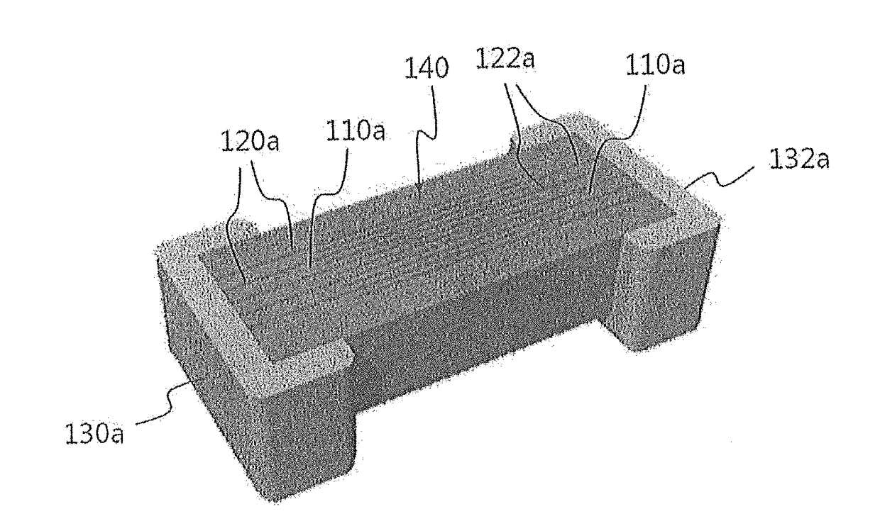
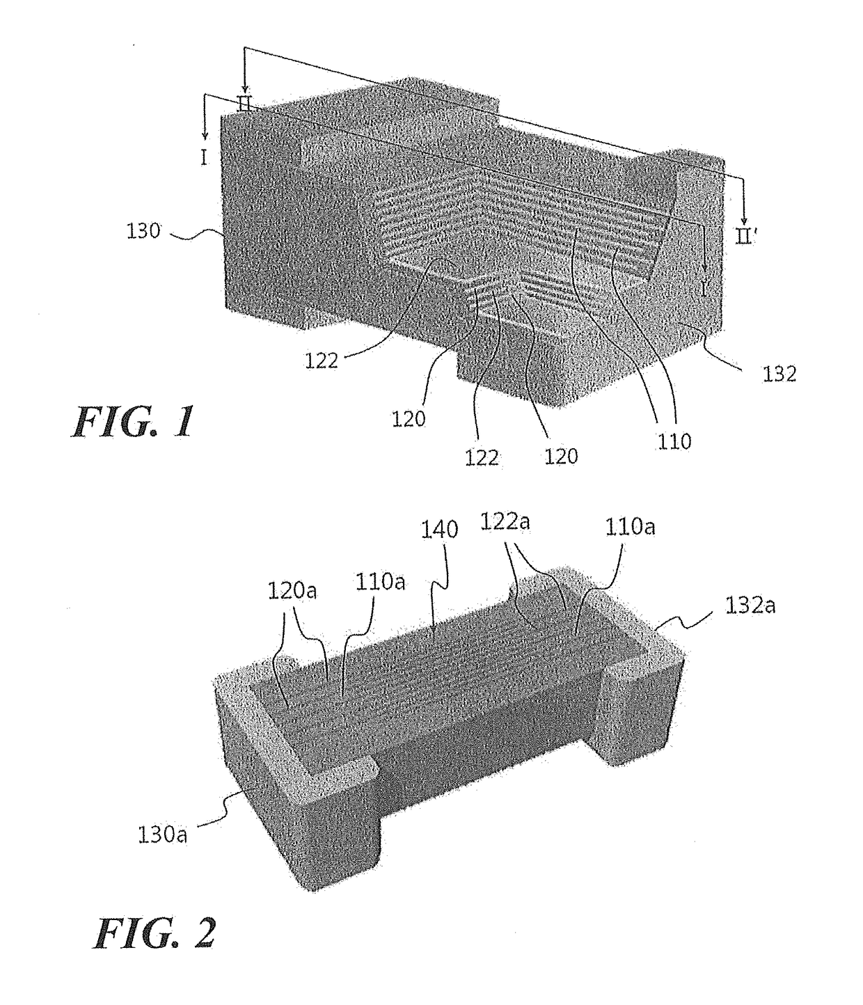
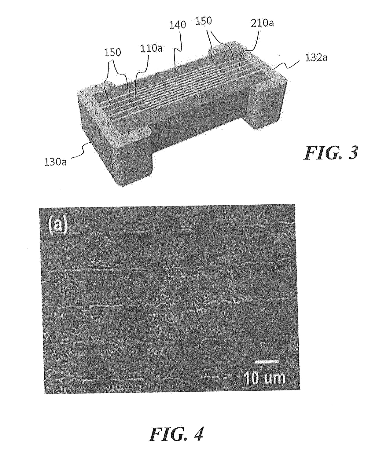
[0161]In order to improve gas sensitivity, the metal films 150 are formed of a conductive metal having a lower contact resistance with a gas sensitive material layer than the internal electrodes 120a and 122a on the internal electrodes 120a and 122a exposed through the sensing surface 140 of the sensor body.

[0162]When a gas sensitive material layer is formed of an oxide semiconductor, CNTs, chalcogens, a chalcogenide, or the like on the internal electrodes 120a and 122a, a metal having a low contact resistance with each gas sensitive material layer may be selected.

[0163]For example, nickel (Ni), which forms the internal electrodes 120a and 122a, is gradually oxidized at room temperature to change electrical properties thereof, and specifically, when the gas sensor is driven at a high temperature, electrode characteristics thereof may be significantly degraded. Therefore, a conductive metal having a low contact resistance with a gas sensitive material layer is plated (or deposited) o...

example 2

[0166]A thin film type or thick film type gas sensor may be prepared by depositing (or applying) a metal or an oxide semiconductor, capable of sensing a gas, as a gas sensitive material on a part or whole of the sensing surface 140 on which the metal films 150 are exposed. The thin film type or thick film type gas sensor has advantages in that manufacturing is simpler and sensitivity is more excellent as compared to a bulk type gas sensor.

[0167]As an example of the thin film type or thick film type gas sensor, an oxide semiconductor gas sensor may be formed by depositing (or applying) an oxide semiconductor as a gas sensitive material on a part or whole of the sensing surface 140 (see FIG. 3) on which the metal films 150 are exposed. FIG. 8 shows a state in which an oxide semiconductor gas sensor is formed by depositing a metal oxide film as a gas sensitive material on the sensing surface 140 (see FIG. 3) on which the metal films 150 are exposed.

[0168]Referring to FIG. 8, a gas sens...

example 3

[0174]A CNT gas sensor may be formed by depositing (applying) CNTs as a gas sensitive material on a part or whole of the sensing surface 140 (see FIG. 3) on which the metal films 150 are exposed.

[0175]The CNTs have a small diameter and a large specific surface area, are susceptible to changes in current flow with only a small amount of gas adsorption, and have good mechanical properties and excellent electrical properties.

[0176]Single-wall carbon nanotubes (SWNTs) or multi-wall carbon nanotubes (MWNTs) may be used as the CNTs. However, the SWNTs are preferably used as the CNTs in consideration of sensitivity of the sensor or the like. The CNTs may be synthesized by a method such as chemical vapor deposition (CVD) or the like. Since a method of synthesizing CNTs is already known, a detailed description thereof will be omitted here. The CNTs used in the CNT gas sensor preferably have a diameter of about 1 to 20 nm and a length of about 1 to 50 μm.

[0177]A suspension in which CNTs are d...


PUM

PropertyMeasurementUnit
frequencyaaaaaaaaaa
temperatureaaaaaaaaaa

Abstract

The present invention relates to a gas sensor and a manufacturing method thereof. A sensor body of the gas sensor is formed by cutting a multi-layered ceramic / metal platform where a plurality of sequential layer structures of a ceramic dielectric material and metal are layered in a layering direction. The sensor body includes at least one layered body wherein a ceramic dielectric material, a first internal electrode, a ceramic dielectric material, and a second internal electrode are sequentially layered. The first internal electrode and the second internal electrode are exposed through a cut surface by cutting. The first internal electrode is electrically connected to a first electrode terminal disposed on a first side of the sensor body, and the second internal electrode is electrically connected to a second electrode terminal disposed on a second side of the sensor body facing the first side. The first and the second internal electrode are exposed to form a sensing surface on at least one side of the sensor body excluding a side where the first and the second electrode terminal are installed. A gas sensing material layer for gas detection is formed on a portion or an entire upper portion of the sensing surface, or a metal film whose contact resistance with the gas sensing material layer is lower than the first and the second internal electrode is formed on upper portions of the first and the second internal electrode which are exposed and a gas sensing material layer for gas detection is formed on a portion or an entire upper portion of the sensing surface where the metal film is formed.

Description

TECHNICAL FIELD[0001]The present invention relates to a gas sensor capable of sensing a gas and a method of manufacturing the same, and more particularly, to a multi-layer ceramic / metal gas sensor, in which it is possible to mass-produce a sensor platform at low cost using a multi-layer ceramic / metal process (MLCP), it is easy to adjust thicknesses and the layered number of internal electrodes made of a metal and ceramic dielectrics, a structure in which internal electrodes spaced apart from each other are separated by ceramic dielectrics may prevent a short circuit and ensure long-term stability, a gas sensitive material layer is formed on a sensing surface on which the internal electrodes are exposed so that sensitivity may be improved, and various types of gas sensitive materials and deposition processes may be applied according to a target gas, and a method of manufacturing the same.BACKGROUND ART[0002]A gas sensor is a device which senses toxic gases, such as NOX, CO, H2S, NH3,...

Claims


Application Information

Patent Timeline
Patent Type & Authority Applications(United States)
IPC IPC(8): G01N27/409B82B3/00B82B1/00
CPCG01N27/409B82B3/0004B82B1/005B82Y15/00G01N27/127B82B1/008B82B3/0038G01N27/407G01N27/4075
Inventor CHOA, YONG HOLIM, HYO RYOUNGCHOI, YO MINEOM, NU SI AKIM, SUNGYOUL
Owner IND UNIV COOPERATION FOUND HANYANG UNIV ERICA CAMPUS
Why Eureka
Try Eureka