
Multilayer ceramic capacitor

a multi-layer ceramic and capacitor technology, applied in the field of multi-layer ceramic capacitors, can solve the problems of poor electrical connection between the the inner electrode, increased risk of sintered first outer electrode being peeled off, etc., to achieve good structural strength, improve quality and yield, and improve the effect of compactness

Active Publication Date: 2018-08-16
HOLY STONE ENTERPRISE
View PDF18 Cites 14 Cited by
  • Summary
  • Abstract
  • Description
  • Claims
  • Application Information

AI Technical Summary

Benefits of technology

The present invention provides a multilayer ceramic capacitor with good structural strength, higher compactness, and improved quality and yield. The ceramic capacitor has a base part and an outer electrode layer. The base part includes ceramic dielectric and inner electrodes. The outer electrode layer is formed at two opposite sides of the base part, with each inner electrode terminal exposed out of one of the two sides of the ceramic dielectric. The first outer electrode is formed by sintering the base part and the ceramic dielectric, and the second outer electrode is formed by metal powder and resin material. The second outer electrode can further be plated to extend the electrical connection. The outer electrode layer has a special multilayer structure to prevent the diffusion of plating solution or other impurities.

Problems solved by technology

If the thickness of the first outer electrode coated is higher than 70 μm, the risk of the sintered first outer electrode being peeled off is increased along with the increasing of the thickness; otherwise, if the thickness is lower than 5 μm, the electrical connection between the sintered first outer electrode and the inner electrode may be poor.

Method used


Image

  • Multilayer ceramic capacitor
  • Multilayer ceramic capacitor
  • Multilayer ceramic capacitor

Examples


Embodiment Construction

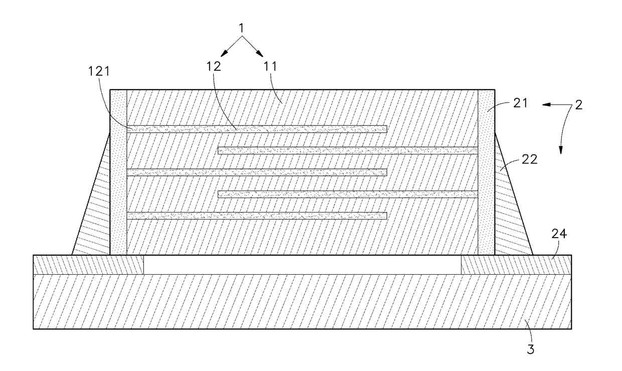
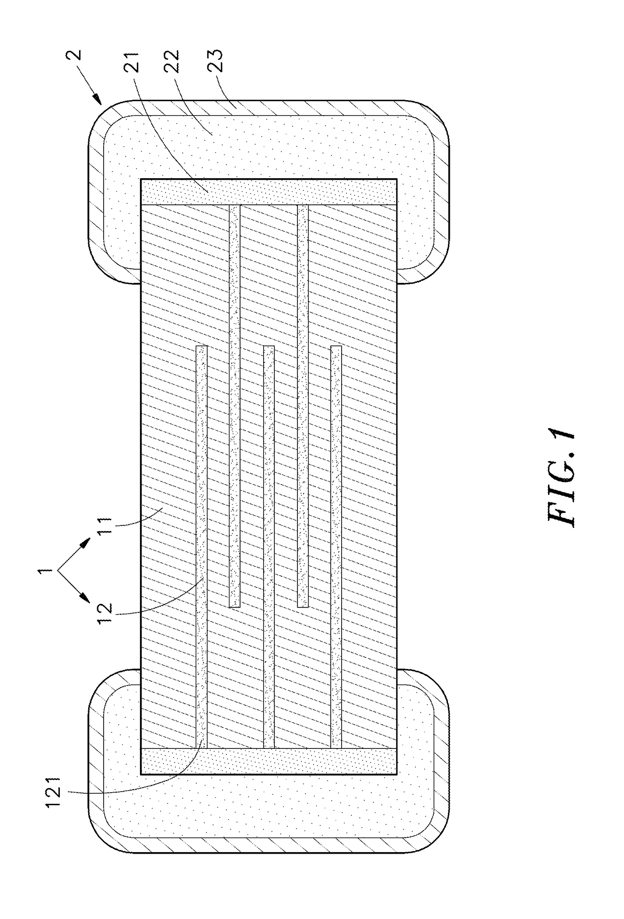
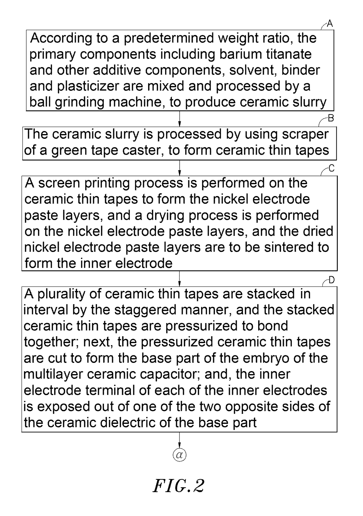
[0028]Please refer to FIGS. 1, 2, 3 and 4, which are sectional side view of a multilayer ceramic capacitor of a preferred embodiment of the present invention, and a first, second and third parts of a flowchart of a method of manufacturing the multilayer ceramic capacitor of the present invention. As shown in FIG. 1, the multilayer ceramic capacitor includes a base part 1 and an outer electrode layer 2 formed on two opposite sides of the base part 1.

[0029]In order to form the base part 1, a plurality of ceramic thin tapes are arranged in interval by a staggered manner, to stack in a multi-layer structure, and the stacked layers are pressurized to bond together, and then cut to form the base part 1 of an embryo of the multilayer ceramic capacitor. The base part 1 includes ceramic dielectric 11 and a plurality of inner electrodes 12 formed inside the ceramic dielectric 11. Each of the inner electrodes 12 includes an inner electrode terminal 121 formed a side thereof and exposed out one...


PUM

PropertyMeasurementUnit
particle sizeaaaaaaaaaa
thicknessaaaaaaaaaa
temperatureaaaaaaaaaa

Abstract

A multilayer ceramic capacitor and a method of manufacturing the same are disclosed. A base part of the multilayer ceramic capacitor includes ceramic dielectric and inner electrodes formed inside the ceramic dielectric, and a terminal of each of the inner electrodes is exposed out of one of the two opposite sides of the base part, to form inner electrode terminals. First outer electrodes are formed on the two sides of the base part and the outside of the inner electrode terminals, and second outer electrodes are formed on the first outer electrodes. The first outer electrodes and the base part are formed together by sintering manner, and the second outer electrodes are formed by metal powder and resin material, thereby solving the problem that the vitreous component diffuses around, or solving the problem that plating solution permeates into the base part or the ceramic dielectric during plating process.

Description

[0001]This application claims the priority benefit of Taiwan patent application number 106102946, filed on Jan. 25, 2017.BACKGROUND OF THE INVENTION1. Field of the Invention[0002]The present disclosure relates to a multilayer ceramic capacitor and a method of manufacturing the same, and more particularly to a multilayer ceramic capacitor including a base part and outer electrode layer formed on two sides of the base part, and the outer electrode layer includes first outer electrodes formed with the base part together by a sintering manner, and second outer electrodes formed by solidifying a mixture of metal powder and resin; the process of forming the first outer electrodes of the outer electrode layer is performed at about 1300° C., and the subsequent process of forming the second outer electrode or the plating process for forming further-outer electrodes is performed at about 250° C. or lower temperature, and the material of the second outer electrode is mixture of resin and metal...

Claims


Application Information

Patent Timeline
Patent Type & Authority Applications(United States)
IPC IPC(8): H01G4/30H01G4/008H01G4/12
CPCH01G4/30H01G4/008H01G4/1227H01G4/248H05K1/181H05K2201/10015H01G4/12H01G4/1209H01G13/00H01G4/232H01G4/2325
Inventor NAGAI, ATSUOCHEN, SHENG-YI
Owner HOLY STONE ENTERPRISE
Learn More