Check patentability & draft patents in minutes with Patsnap Eureka AI!

Circuit topology of memory chips with embedded function test pattern generation module connected to normal access port physical layer

a technology of function test pattern and circuit topology, applied in the field of memory architecture, can solve problems such as the challenge of wafer level testing

Active Publication Date: 2018-08-23
PIECEMAKERS TECH
View PDF9 Cites 0 Cited by
  • Summary
  • Abstract
  • Description
  • Claims
  • Application Information

AI Technical Summary

Benefits of technology

The proposed memory chip architecture allows for testing the operation of a chip through normal access interface pads, rather than using extra testing paths. This results in a test result that is the same as a control chip / system that is externally connected to the chip. Both the proposed chip and the control chip / system use the normal access interface pads, so the testing behavior of the proposed chip is similar to that of the control chip / system.

Problems solved by technology

As the configuration of memories has hundreds of interface pads, it would be a challenge to do wafer level testing due to its high pad counts.

Method used


Image

  • Circuit topology of memory chips with embedded function test pattern generation module connected to normal access port physical layer
  • Circuit topology of memory chips with embedded function test pattern generation module connected to normal access port physical layer
  • Circuit topology of memory chips with embedded function test pattern generation module connected to normal access port physical layer

Examples


Embodiment Construction

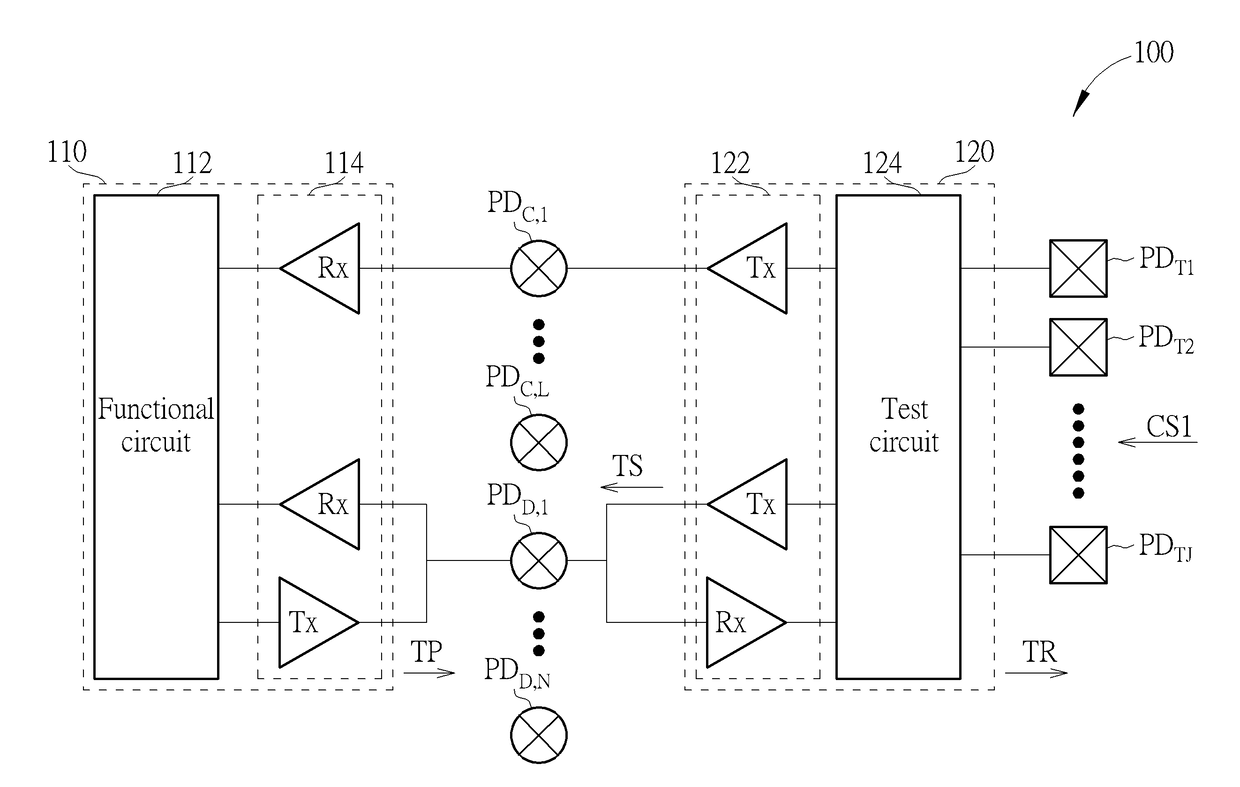
[0011]The proposed circuit topology of memory chips with an embedded function test pattern generation module connected to an access PHY (i.e. a normal access PHY) may include a function block, an embedded test block (i.e. the embedded function test pattern generation module) and a plurality of interface pads (or regular interface pads), wherein the circuit topology receives and outputs signals through the normal access PHY. Additionally, the embedded test block (or a test circuit of the embedded test block) transmits a test signal through the interface pads to test the function block (or a functional circuit of the function block) rather than tests the function block through extra paths. By way of example but not limitation, the test signal generated from the embedded test block and control signal (s) generated from a control chip or a control system may be transmitted only through the interface pads / the access PHY. Hence, a test result corresponding to a test pattern generated by t...


PUM


Abstract

A memory chip architecture includes a plurality of test pads, a plurality of interface pads, a function block and an embedded test block. The function block is coupled to the interface pads. The embedded test block is coupled to the test pads. The embedded test block is connected to an access port physical layer (PHY) through the interface pads. The interface pads are disposed between the function block and the embedded test block. The embedded test block is arranged for generating at least one test pattern as a test signal, and outputting the test signal to the function block through the interface pads to test the function block.

Description

BACKGROUND OF THE INVENTION1. Field of the Invention[0001]The disclosed embodiments of the present invention relate to a memory architecture, and more particularly, to a circuit topology of memory chips with an embedded function test pattern generation module connected to a normal access PHY (Port Physical Layer) / regular interface pads, which transmits a test signal to a chip including a functional circuit through a plurality of the regular interface pads.2. Description of the Prior Art[0002]In high-performance computing and graphics applications, demand for higher bandwidth DRAM continues to increase. Memories with large number of I / O pins have been developed for the demand in years, such as High Bandwidth Memory (HBM) and Wide I / O DRAM. As the configuration of memories has hundreds of interface pads, it would be a challenge to do wafer level testing due to its high pad counts. Normally, in addition to the exiting interface pads of the memory, an extra test pad interface is equippe...

Claims


Application Information

Patent Timeline
IPC IPC(8): G11C29/12G11C29/36
CPCG11C29/1201G11C2029/3602G11C29/36G11C29/04G11C29/12G11C2029/0409G11C2029/1206G11C29/48
Inventor WANG, GYH-BINWANG, CHUN-KAI
Owner PIECEMAKERS TECH
Features
  • R&D
  • Intellectual Property
  • Life Sciences
  • Materials
  • Tech Scout
  • Unparalleled Data Quality
  • Higher Quality Content
  • 60% Fewer Hallucinations
Learn More