Triangle hatch pattern for additive manufacturing

a technology of additive manufacturing and triangles, which is applied in the direction of additive manufacturing, manufacturing tools, additive manufacturing, etc., can solve the problems of slow build process, melt pattern inaccuracy, burnout effect, etc., and achieve the desired speed of the build process, improve the microstructure of the completed component, and improve the build efficiency and/or stress balance

Active Publication Date: 2018-09-06
GENERAL ELECTRIC CO
View PDF4 Cites 25 Cited by
  • Summary
  • Abstract
  • Description
  • Claims
  • Application Information

AI Technical Summary

Benefits of technology

[0014]The disclosure relates to an improved scanning strategy, having a hatch pattern for scanning a laser during an AM build process. When controlling the laser during the build process according to one embodiment, an alternating hatch pattern is used to form solidification lines on each layer so as to improve the microstructure of the completed component. In one aspect, a first layer is formed by scanning a laser across the surface of the powder to form at least partially melted solidification lines, wherein each line is scanned and formed as a solidification line forming two angled segments of a triangle. In other words, a solidification line is formed along a first liner path and a second linear path and the first and second linear paths are angled with respect to one another. The first and second linear paths of the laser scan and subsequently formed solidification lines may be contained within a stripe region forming a portion of the component being built. Once the series of solidification lines are formed on the layer, a subsequent layer of powder is added on top of the previously solidified scan lines; and a second series of solidification lines are formed as a first linear path and a second linear path, wherein the first linear path is angled with relation to the second liner path. Further, the abovementioned angle formed between the first linear path and second linear path may be varied for each subsequent layer; so that no subsequent layer has the same angle between the first linear path and the second linear path, thereby improving build efficiency and / or the balance of stresses imparted in the finished solidified component formed using the AM process.
[0015]By dividing up areas of the surface to be scanned as described below, further variance between layers can be achieved during an AM build allowing for increased control of the microstructure of the completed component. Build efficiency can also be further increased by preventing unnecessary jumps of the energy source, preventing unnecessary on / off transitions of the laser and / or by improving control and / or efficiency of heat buildup within the layer being formed and / or the layers of the build. In the case of multiple lasers and / or energy sources being used, the disclosed scanning scheme may be used to further improve the AM build by employing various strategies for the use of multiple energy sources (e.g. lasers and / or electron-beams).
[0016]When forming a series of the abovementioned first solidification line and second solidification lines. The possibility of a high energy density region may occur near the end of a stripe or near the end of contour of the component, in order to balance the heat distribution throughout the layer, a third series of solidification lines may be formed that are substantially parallel to a first series of solidification lines and intersect one of the second solidification lines. By forming the third series of solidification lines, the distance over which the energy source is scanned is increased, thus preventing a high concentration of heat within a certain region of the component being built. By dividing up areas of the surface to be scanned as described below, further variance between layers can be achieved during an AM build allowing for increased control of the microstructure of the completed component. Build efficiency can also be further increased by preventing unnecessary jumps of the energy source, preventing unnecessary on / off transitions of the laser and / or by improving control and / or efficiency of heat buildup within the layers of the build. In the case of multiple lasers and / or energy sources being used, the disclosed scanning scheme may be used to further improve the AM build by employing various strategies for the use of multiple energy sources (e.g. lasers and / or electron-beams).

Problems solved by technology

One challenge associated with laser based AM is producing a desired melt pattern in the powder while maintaining a desired speed of the build process.
Slowing of the build process and / or inaccuracies in the melt pattern result, for example, when a laser is turned on and / or off too early or late at the beginning and / or end of a hatch line.
Turning a laser on too early may result in a burn-in effect where the melt pool is longer than the desired length of the hatch.
Further, the buildup of heat within the powder and fused material during a build is a concern, as various material defects may occur if too much heat is built up in the material during an AM process and / or if insufficient heat is built up to properly fuse the powder.

Method used


Image

  • Triangle hatch pattern for additive manufacturing
  • Triangle hatch pattern for additive manufacturing
  • Triangle hatch pattern for additive manufacturing

Examples


Embodiment Construction

[0034]While the aspects described herein have been described in conjunction with the example aspects outlined above, various alternatives, modifications, variations, improvements, and / or substantial equivalents, whether known or that are or may be presently unforeseen, may become apparent to those having at least ordinary skill in the art. Accordingly, the example aspects, as set forth above, are intended to be illustrative, not limiting. Various changes may be made without departing from the spirit and scope of the disclosure. Therefore, the disclosure is intended to embrace all known or later-developed alternatives, modifications, variations, improvements, and / or substantial equivalents.

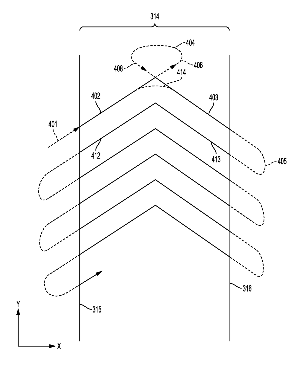
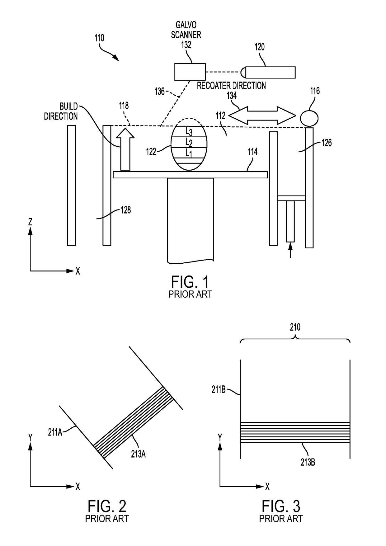
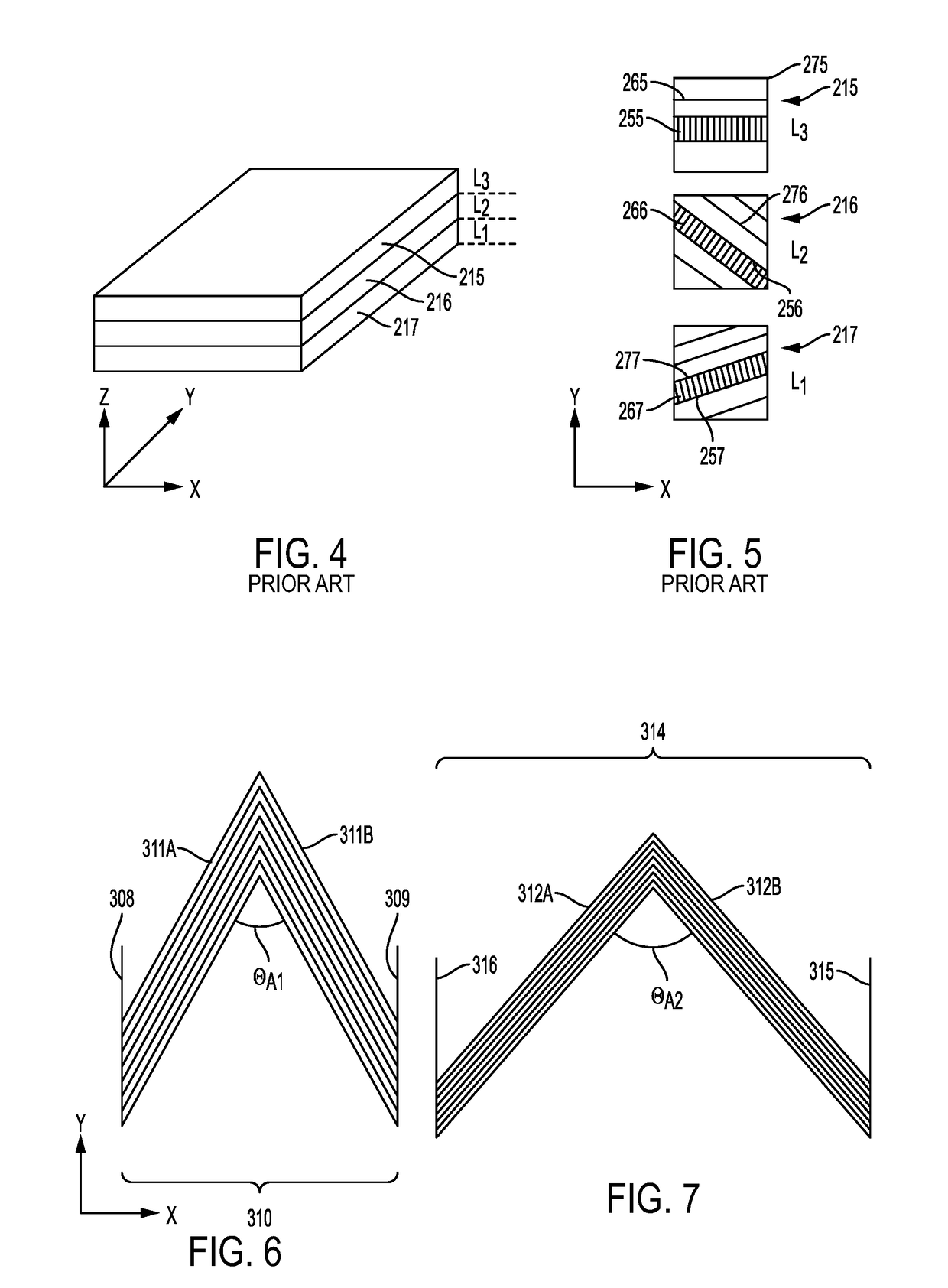
[0035]When using any of the abovementioned AM techniques to form a part by at least partially melting a powder, a scan of the laser across the powder material, in a raster scan fashion is used to create hatch scans (hereinafter referred to interchangeably as hatch scans, rasters, scan lines, or sol...


PUM

PropertyMeasurementUnit
angleaaaaaaaaaa
angleaaaaaaaaaa
angleaaaaaaaaaa

Abstract

A scanning technique for the additive manufacturing of an object. The method comprises the irradiation of a portion of a given layer of powder to form a fused region using an energy source. When forming an object layer by layer, the irradiation follows a first irradiation path bounded by a first stripe, wherein the first irradiation path is formed at an oblique angle with respect to the first stripe. The first irradiation path further comprises at least a first scan vector and a second scan vector at least partially melting a powder and forming a first solidification line and second solidification line respectively, wherein the first solidification intersects and forms an oblique angle with respect to the second solidification line. After a layer is completed, a subsequent layer of powder is provided over the completed layer, and the subsequent layer of powder is irradiated. Irradiation of the subsequent layer of powder follows a second irradiation path bounded by a second stripe. wherein the second irradiation path is formed at an oblique angle with respect to the second stripe. The first irradiation path further comprises at least a third scan vector and a fourth scan vector at least partially melting a powder and forming a third solidification line and fourth solidification line respectively, wherein the third solidification intersects and forms an oblique angle with respect to the fourth solidification line

Description

INTRODUCTION[0001]The disclosure relates to an improved method of producing components using an additive manufacturing technique. The disclosure provides an improved method of producing components, some of examples of which comprise: improved microstructure, decreased manufacturing time, decreased cost, decreased waste of materials. In particular, the disclosure relates to a process of scanning an energy beam (i.e., laser or e-beam) during a powder-based additive manufacturing build process.BACKGROUND[0002]Additive manufacturing (AM) techniques may include electron beam freeform fabrication, laser metal deposition (LMD), laser wire metal deposition (LMD-w), gas metal arc-welding, laser engineered net shaping (LENS), laser sintering (SLS), direct metal laser sintering (DMLS), electron beam melting (EBM), powder-fed directed-energy deposition (DED), and three dimensional printing (3DP), as examples. AM processes generally involve the buildup of one or more materials to make a net or n...

Claims


Application Information

Patent Timeline
Patent Type & Authority Applications(United States)
IPC IPC(8): B22F3/105B33Y10/00B33Y30/00B33Y50/02B23K26/342B23K15/00B23K26/082
CPCB22F3/1055B33Y10/00B33Y30/00B33Y50/02B22F2003/1057B23K15/0086B23K26/082B22F2003/1056B23K26/342Y02P10/25B29C64/153B22F12/49B22F12/45B22F12/63B22F10/36B22F10/28B22F12/41B22F12/224B22F10/00
Inventor MAMRAK, JUSTINREDDING, MACKENZIE RYAN
Owner GENERAL ELECTRIC CO
Why Eureka
Try Eureka