Semiconductor power module and power conversion apparatus

a technology of power conversion apparatus and semiconductor, applied in the direction of semiconductor devices, solid-state devices, basic electric elements, etc., can solve the problem of sub-electrode destruction, and achieve the effect of improving reliability

Active Publication Date: 2018-09-06
MITSUBISHI ELECTRIC CORP
View PDF5 Cites 5 Cited by
  • Summary
  • Abstract
  • Description
  • Claims
  • Application Information

AI Technical Summary

Benefits of technology

[0006]In the present invention, the substrate electrode is embedded in the concave portion of the insulating substrate. This avoids any level difference between the insulating substrate and the substrate electrode, and makes it possible to uniformly form the insulating resin on the surface of the substrate electrode and securely cover the top end part of the substrate electrode with the insulating resin. It is therefore possible to improve reliability with respect to a withstand voltage.

Problems solved by technology

However, a top end part of the substrate electrode is not covered with the insulating resin due to surface tension of resin after the application of the insulating resin or volume contraction when the resin is caused to harden.
As a result, current leakage occurs between the substrate electrodes, abnormal discharge takes place at the top end part of the substrate electrode, causing a problem that the substrate electrode is destroyed.

Method used


Image

  • Semiconductor power module and power conversion apparatus
  • Semiconductor power module and power conversion apparatus
  • Semiconductor power module and power conversion apparatus

Examples


first embodiment

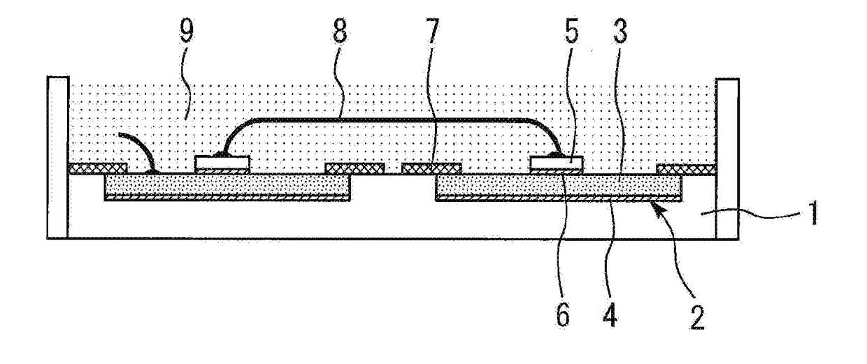
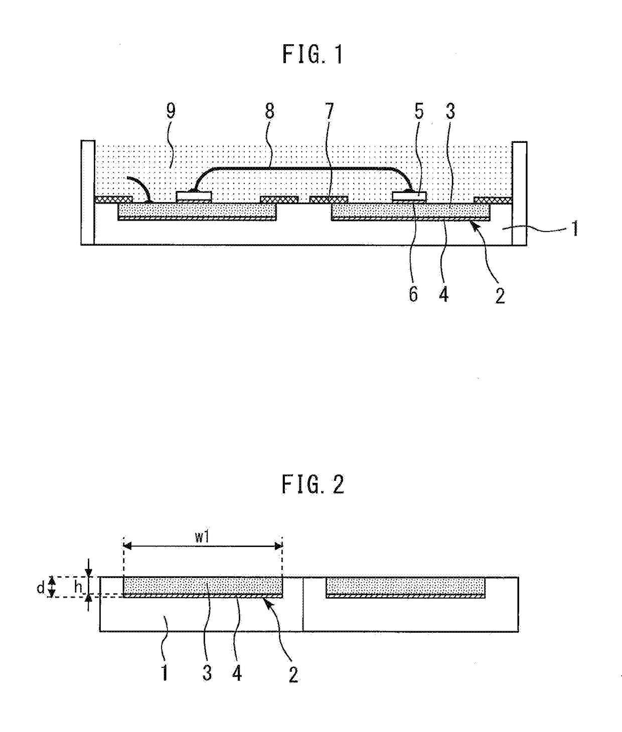
[0018]FIG. 1 is a cross-sectional view illustrating a semiconductor power module according to a first embodiment of the present invention. A concave portion 2 is formed on a top surface of an insulating substrate 1 of ceramic or the like. A substrate electrode 3 is embedded in the concave portion 2 via solder 4. FIG. 2 is an enlarged cross-sectional view of the insulating substrate and the substrate electrode according to the first embodiment of the present invention. The substrate electrode 3 has a thickness h of 200 μm to 800 μm, which is equal to or less than a depth d of the concave portion 2.

[0019]A semiconductor device 5 is bonded onto the substrate electrode 3 via solder 6. A polyimide-based or polyamide-imide-based insulating resin 7 having a thickness of 5 μm to 100 μm covers the top end part of the substrate electrode 3. A wire-interconnect 8 for applying a voltage is connected to the top surface of the semiconductor device 5. Silicone gel 9 covers the substrate electrode ...

second embodiment

[0025]FIG. 10 is a cross-sectional view illustrating a semiconductor power module according to a second embodiment of the present invention. FIG. 11 is an enlarged cross-sectional view of an insulating substrate and a substrate electrode according to the second embodiment of the present invention. Unlike the first embodiment, a width w2 of the substrate electrode 3 is smaller than a width wl of the concave portion 2. The insulating resin 7 covers the top end part and the side face as well of the substrate electrode 3. A thickness of the insulating resin 7 is smaller than (w1=w2) / 2. The rest of the configuration is similar to that of the first embodiment.

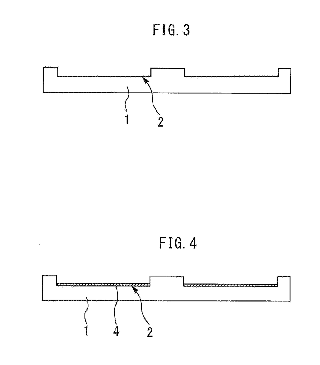
[0026]Next, a method of manufacturing the semiconductor power module according to the present embodiment will be described. FIGS. 12 to 14 are cross-sectional views illustrating the method of manufacturing the semiconductor power module according to the second embodiment of the present invention. First, steps in FIG. 3 and FIG. 4 wil...

third embodiment

[0030]In this embodiment, the semiconductor power module according to the first or second embodiment described above are applied to an electric power conversion device. The electric power conversion device is, for example, an inverter device, a converter device, a servo amplifier, or a power supply unit. Although the present invention is not limited to a specific electric power conversion device, a case where the present invention is applied to a three-phase inverter will be described below.

[0031]FIG. 15 is a block diagram illustrating a configuration of an electric power conversion system to which the electric power conversion device according to the third embodiment of the present invention is applied. This electric power conversion system includes a power supply 100, an electric power conversion device 200, and a load 300. The power supply 100 is a DC power supply and supplies DC power to the electric power conversion device 200. The power supply 100 can be composed of various co...


PUM


Abstract

A semiconductor power module includes: an insulating substrate including a concave portion provided on a top surface of the insulating substrate; a substrate electrode embedded in the concave portion; a semiconductor device bonded onto the substrate electrode; and an insulating resin covering a top end part of the substrate electrode.

Description

BACKGROUND OF THE INVENTIONField[0001]The present invention relates to a semiconductor power module and a power conversion apparatus.Background[0002]Semiconductor power modules are required to exhibit high reliability to be able to consecutively turn on / off a current at a high voltage for a long period of time. In order to improve reliability with respect to a withstand voltage, substrate electrodes are covered with insulating resin and current leakage is thereby suppressed. For example, a thin film of polyimide-based or polyamide-imide-based insulating resin is applied to the surfaces of the substrate electrodes on a ceramic insulating substrate and hardened to thereby improve reliability with respect to a withstand voltage (e.g., see JP 2006-32617 A).SUMMARY[0003]Insulating resin having a thickness of 5 μm to 100 μm is applied using a potting method. However, a top end part of the substrate electrode is not covered with the insulating resin due to surface tension of resin after th...

Claims


Application Information

Patent Timeline
Patent Type & Authority Applications(United States)
IPC IPC(8): H01L23/08H01L23/057H01L23/13H01L23/00H01L21/48H02M7/00
CPCH01L23/08H01L23/057H01L23/13H01L24/48H01L21/481H02M7/003H01L2224/48137H02P27/08H01L23/3107H01L23/3121H01L23/24H01L23/3135H01L23/49827H01L2924/00014H01L2924/19107H01L2224/291H01L2224/32225H01L2224/92247H01L24/29H01L24/32H01L2924/1511H01L2924/1517H01L25/072H01L2224/45099H01L2924/014
Inventor KUGA, SHOICHI
Owner MITSUBISHI ELECTRIC CORP
Why Eureka
Try Eureka