Oxide film removing method, oxide film removing apparatus, contact forming method, and contact forming system

Inactive Publication Date: 2018-09-13
TOKYO ELECTRON LTD
View PDF14 Cites 10 Cited by
  • Summary
  • Abstract
  • Description
  • Claims
  • Application Information

AI Technical Summary

Problems solved by technology

Further, since the structure of the source and drain portions of the fin FET is complicated, a chemical oxide removal (COR) processing is considered as a processing capable of removing the natural oxide film in a portion where ions hardly reach.

Method used


Image

  • Oxide film removing method, oxide film removing apparatus, contact forming method, and contact forming system
  • Oxide film removing method, oxide film removing apparatus, contact forming method, and contact forming system
  • Oxide film removing method, oxide film removing apparatus, contact forming method, and contact forming system

Examples


first exemplary embodiment

[0074][Oxide Film Removing Method]

[0075]First, an oxide film removing method according to a first exemplary embodiment will be described.

[0076]FIG. 1 is a flowchart illustrating an oxide film removing method according to a first exemplary embodiment. FIGS. 2A to 2D are sectional views illustrating the oxide film removing method step by step.

[0077]In the exemplary embodiment, descriptions will be made on a case of removing a natural oxide film formed on the surface of a silicon portion of the bottom of a trench formed as a predetermined pattern in a workpiece before forming a contact by depositing a contact metal on the silicon portion.

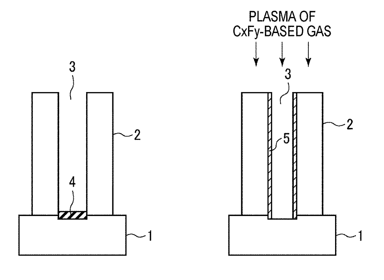
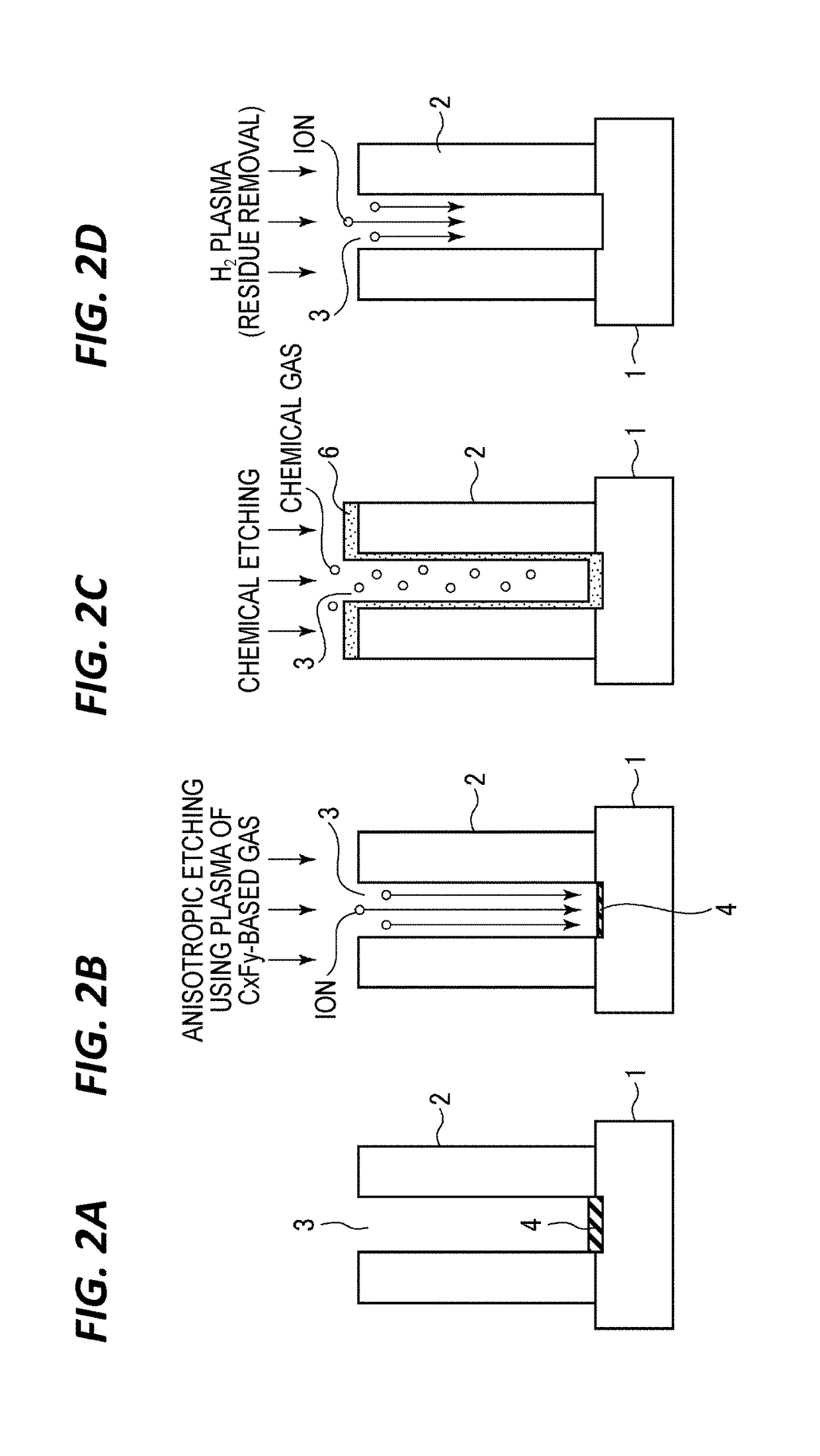
[0078]First, a processing target substrate (silicon wafer) having an insulating film 2 formed on a silicon base 1 and a trench 3 formed as a predetermined pattern in the insulating film 2 is prepared (step 1; FIG. 2A). A natural oxide film (silicon-containing oxide film) 4 is formed on the silicon portion of the bottom of the trench 3. The insulating f...

second exemplary embodiment

[0155]Next, an oxide film removing method according to a second exemplary embodiment will be described.

[0156]FIG. 11 is a flowchart illustrating an oxide film removing method according to a second exemplary embodiment. FIGS. 12A to 12D are sectional views illustrating the oxide film removing method step by step.

[0157]Also in the exemplary embodiment, descriptions will be made on a case of removing a natural oxide film formed on the surface of a silicon portion of the bottom of a trench formed as a predetermined pattern in a workpiece before forming a contact by depositing a contact metal on the silicon portion.

[0158]First, a processing target substrate (silicon wafer) having an insulating film 2 formed on a silicon base 1 and a trench 3 formed as a predetermined pattern in the insulating film 2 is prepared (step 21; FIG. 12A). A natural oxide film (silicon-containing oxide film) 4 is formed on the silicon portion on the bottom of the trench 3. The insulating film 2 is mainly made of...

third exemplary embodiment

[0198]Next, an oxide film removing method according to a third exemplary embodiment will be described.

[0199]FIG. 21 is a flowchart illustrating an oxide film removing method according to a third exemplary embodiment. FIGS. 22A to 22C are sectional views illustrating the oxide film removing method step by step.

[0200]Also in the exemplary embodiment, descriptions will be made on a case of removing a natural oxide film formed on the surface of a silicon portion of the bottom of a trench formed as a predetermined pattern in a workpiece before forming a contact by depositing a contact metal on the silicon portion.

[0201]First, a processing target substrate (silicon wafer) having an insulating film 2 formed on a silicon base 1 and a trench 3 formed as a predetermined pattern in the insulating film 2 is prepared (step 31; FIG. 22A). A natural oxide film (silicon-containing oxide film) 4 is formed on the silicon portion on the bottom of the trench 3. The insulating film 2 is mainly made of a...


PUM


Abstract

Disclosed is a method for removing, from a processing target substrate having an insulating film with a predetermined pattern formed thereon, a silicon-containing oxide film formed in a silicon portion of a bottom of the pattern. The method includes: removing the silicon-containing oxide film formed on the bottom of the pattern by ionic anisotropic plasma etching using plasma of a carbon-based gas; removing a remaining portion of the silicon-containing oxide film after the anisotropic plasma etching, by chemical etching; and removing a residue remaining after the chemical etching.

Description

CROSS-REFERENCE TO RELATED APPLICATIONS[0001]This application is based on and claims priority from Japanese Patent Application Nos. 2017-043853 and 2017-138968 filed on Mar. 8, 2017 and Jul. 18, 2017, respectively, with the Japan Patent Office, the disclosures of which are incorporated herein in their entirety by reference.TECHNICAL FIELD[0002]The present disclosure relates to an oxide film removing method, an oxide film removing apparatus, a contact forming method, and a contact forming system.BACKGROUND[0003]In a case of forming a contact made of silicide on a silicon surface of the bottom of a pattern (e.g., a contact hole or a trench), it is necessary to remove any natural oxide film formed on the silicon surface. Thus, anisotropic etching by ionic etching has been known as a technique for removing the natural oxide film on the bottom of the pattern (see, e.g., Japanese Patent Laid-Open Publication No. 2003-324108).[0004]Meanwhile, for example, in a fin-type channel field effect...

Claims


Application Information

Patent Timeline
Patent Type & Authority Applications(United States)
IPC IPC(8): H01L21/311H01L21/02H01L29/66H01L21/67H01L21/285H01L21/677H01L29/45
CPCH01L21/31116H01L21/02063H01L29/66795H01L21/67069H01L21/28518H01L21/67739H01L21/67167H01L29/456H01L21/30604H01L21/3065H01L21/02057H01L21/67201H01J37/32449H01J37/32816H01J37/32834H01L21/76814H01L29/7853
Inventor KOBAYASHI, TAKASHISAKUMA, TAKASHIYAMASAKI, HIDEAKISHIMIZU, RIOTSUDA, EINOSUKE
Owner TOKYO ELECTRON LTD
Why Eureka
Try Eureka