

High resistivity silicon-on-insulator substrate comprising a charge trapping layer formed by he-n2 co-implantation
a silicon-on-insulator substrate and high-resistance technology, which is applied in the direction of basic electric elements, semiconductor/solid-state device manufacturing, electric apparatus, etc., can solve the problems of wasting one of the substrates, not having suitable thickness uniformity, and time-consuming and costly methods
- Summary
- Abstract
- Description
- Claims
- Application Information
AI Technical Summary
Benefits of technology
Problems solved by technology
Method used
Image

Examples
Embodiment Construction
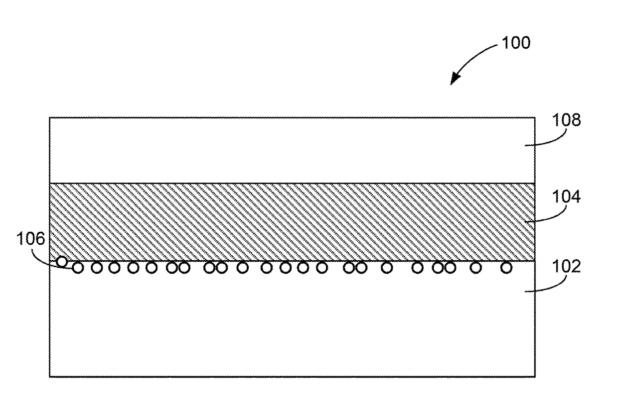
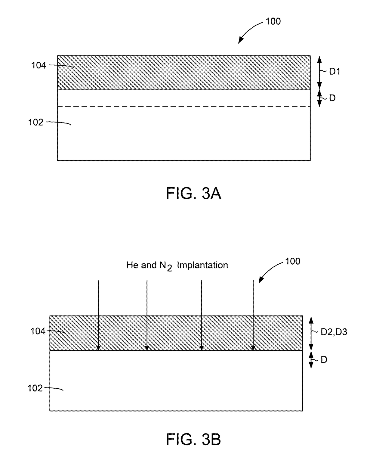
[0020]According to the present invention, a method is provided for preparing a semiconductor-on-insulator composite structure comprising a charge trapping layer (CTL). The present invention is further directed to a semiconductor-on-insulator composite structure comprising a charge trapping layer (CTL). In some embodiments, the semiconductor-on-insulator (e.g., silicon-on-insulator) comprises a high resistivity handle substrate prepared by He—N2 co-implantation and heat treatment to thereby form the charge trapping layer comprising a region of nanovoids. It has been discovered that a charge trapping layer prepared by He—N2 co-implantation and heat treatment, and thus having nanovoids, may suppress the parasitic conduction phenomenon in HR-SOI wafers for RF applications. Co-implantation of He and N2 followed by a heat treatment creates nanometer-size voids at the BOX / handle interface that are electrically activated deep level traps. He implantation followed by heat treatment causes He...
PUM
 Abstract
Description
Claims
Application Information