
Systems and methods for improved collimation sensitivity

a collimation sensitivity and collimation method technology, applied in the direction of radiation generation arrangement, instruments, radioation controlled devices, etc., can solve the problems of limiting the usable area, the size of the detector head, and the conventional approach may not provide the desired or required sensitivity

Active Publication Date: 2018-11-15
GENERAL ELECTRIC CO
View PDF0 Cites 4 Cited by
  • Summary
  • Abstract
  • Description
  • Claims
  • Application Information

AI Technical Summary

Benefits of technology

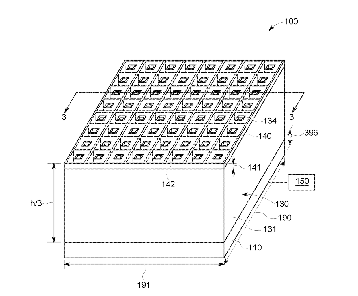
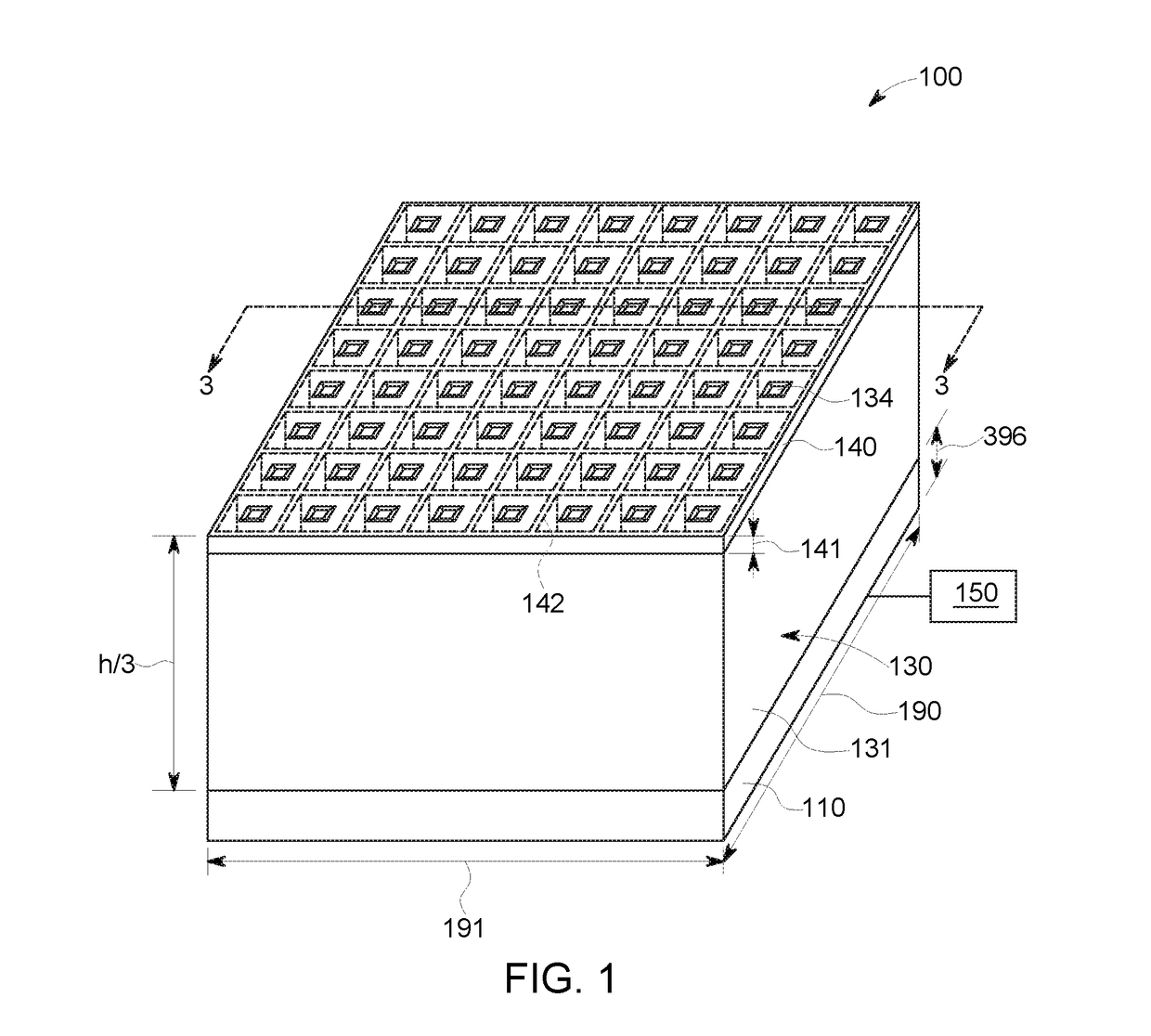
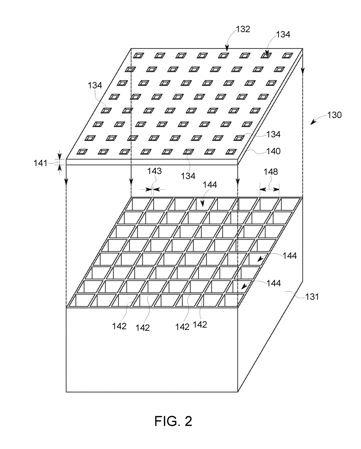
This patent describes a detector assembly that includes a semiconductor detector, a pinhole collimator, and a processing unit. The detector has pixels and the collimator has small openings that correspond to pixels. The processing unit identifies detected events within virtual sub-pixels distributed along the detector's length and width. Each pixel includes multiple virtual sub-pixels, and absorbed photons are counted as events in a corresponding virtual sub-pixel. This allows for more accurate detection and analysis of the radiation incident on the detector. The technical effect of this invention is improved precision and accuracy in detecting radiation.

Problems solved by technology

The size of the detector heads may limit an available usable area for the placement of detectors, such as Cadmium Zinc Telluride (CZT) wafers.
Such conventional approaches may not provide a desired or required sensitivity.

Method used


Image

  • Systems and methods for improved collimation sensitivity
  • Systems and methods for improved collimation sensitivity
  • Systems and methods for improved collimation sensitivity

Examples


Embodiment Construction

[0016]The following detailed description of certain embodiments will be better understood when read in conjunction with the appended drawings. To the extent that the figures illustrate diagrams of the functional blocks of various embodiments, the functional blocks are not necessarily indicative of the division between hardware circuitry. For example, one or more of the functional blocks (e.g., processors or memories) may be implemented in a single piece of hardware (e.g., a general purpose signal processor or a block of random access memory, hard disk, or the like) or multiple pieces of hardware. Similarly, the programs may be stand alone programs, may be incorporated as subroutines in an operating system, may be functions in an installed software package, and the like. It should be understood that the various embodiments are not limited to the arrangements and instrumentality shown in the drawings.

[0017]As used herein, the terms “system,”“unit,” or “module” may include a hardware a...


PUM


Abstract

A detector assembly is provided that includes a semiconductor detector, a pinhole collimator, and a processing unit. The semiconductor detector has a first surface and a second surface opposed to each other. The first surface includes pixels, and the second surface includes a cathode electrode. The pinhole collimator includes an array of pinhole openings corresponding to the pixels. Each pinhole opening is associated with a single pixel of the semiconductor detector, and the area of each pinhole opening is smaller than a corresponding area of the corresponding pixel. The processing unit is operably coupled to the semiconductor detector and configured to identify detected events within virtual sub-pixels distributed along a length and width of the semiconductor detector. Each pixel includes a plurality of corresponding virtual sub-pixels (as interpreted by the processing unit), wherein absorbed photons are counted as events in a corresponding virtual sub-pixel.

Description

BACKGROUND OF THE INVENTION[0001]The subject matter disclosed herein relates generally to apparatus and methods for diagnostic medical imaging, such as Nuclear Medicine (NM) imaging.[0002]In NM imaging, systems with multiple detectors or detector heads may be used to image a subject, such as to scan a region of interest. For example, the detectors may be positioned adjacent the subject to acquire NM data, which is used to generate a three-dimensional (3D) image of the subject.[0003]Single Photon Emission Computed Tomography (SPECT) systems may have moving detector heads, such as gamma detectors positioned to focus on a region of interest. For example, a number of gamma cameras may be moved (e.g., rotated) to different angular positions for acquiring image data. The acquired image data is then used to generate the 3D images.[0004]The size of the detector heads may limit an available usable area for the placement of detectors, such as Cadmium Zinc Telluride (CZT) wafers. The sensitivi...

Claims


Application Information

Patent Timeline
Patent Type & Authority Applications(United States)
IPC IPC(8): G01T1/16H01L27/144H01L31/0296
CPCG01T1/16H01L31/0296H01L27/1446A61B6/40A61B6/42G01T1/244G01T1/249
Inventor SHAHAR, ARIE
Owner GENERAL ELECTRIC CO
Learn More