Supercharge Your Innovation With Domain-Expert AI Agents!

3D semiconductor device and structure

a semiconductor and three-dimensional technology, applied in semiconductor devices, semiconductor/solid-state device details, electrical equipment, etc., can solve the problems of heat removal, deformation of the wire (interconnect) that connects the transistors together, and deformation of the transistors, etc., to achieve significant heat removal and power density reduction, and achieve the effect of reducing the cost of the devi

Inactive Publication Date: 2018-11-15
MONOLITHIC 3D
View PDF0 Cites 8 Cited by
  • Summary
  • Abstract
  • Description
  • Claims
  • Application Information

AI Technical Summary

Benefits of technology

This patent describes a method for making a three-dimensional integrated circuit (3D IC) device. The device includes a first layer with first transistors, a metal layer that connects the transistors, a second layer with second transistors, a third layer with third transistors, and a top metal layer. The first transistors are connected to first circuits through a first set of connections, while the second transistors are connected to second circuits through a second set of connections. The first set of connections includes a through silicon via (TSV), and the second set of connections includes a section of the third transistors. The device also includes a first memory array with a first portion of second transistors and a second memory array with a section of third transistors. The technical effect of this patent is to provide a more efficient and effective method for making 3D IC devices with improved performance and reliability.

Problems solved by technology

However, wires (interconnects) that connect together transistors degrade in performance with “scaling”.
Regardless of the technique used to construct 3D stacked integrated circuits or chips, heat removal is a serious issue for this technology.
Removing the heat produced due to this power density is a significant challenge.
In addition, many heat producing regions in 3D stacked integrated circuits or chips have a high thermal resistance to the heat sink, and this makes heat removal even more difficult.

Method used


Image

  • 3D semiconductor device and structure
  • 3D semiconductor device and structure
  • 3D semiconductor device and structure

Examples


Embodiment Construction

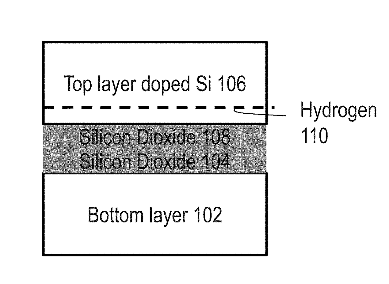
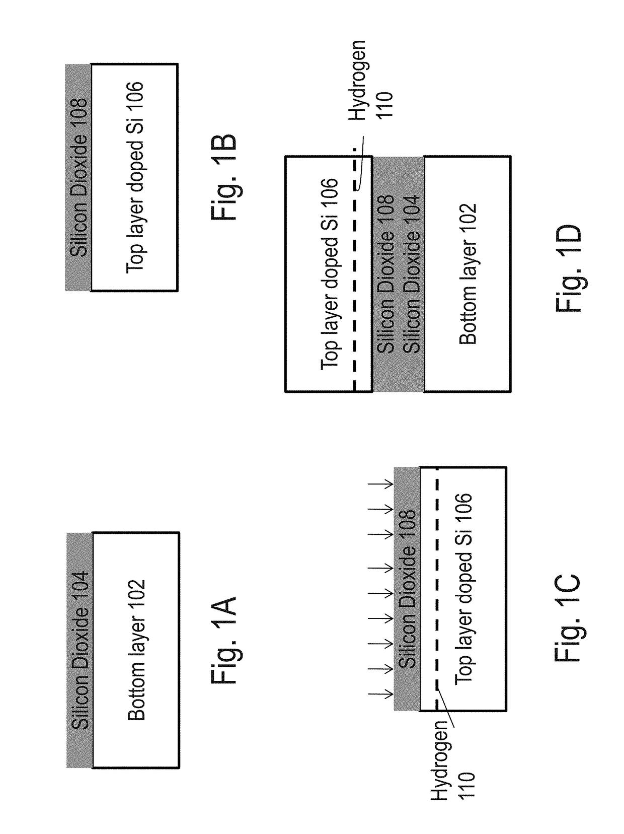
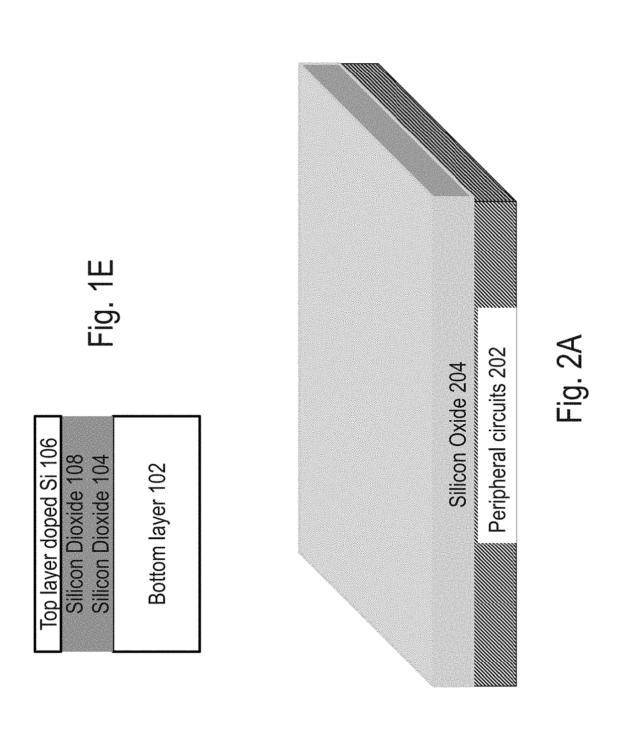
[0030]Various embodiments of inventions are now described with reference to the drawing figures. Persons of ordinary skill in the art will appreciate that the description and figures illustrate rather than limit the invention and that in general the figures are not drawn to scale for clarity of presentation. Such skilled persons will also realize that many more embodiments are possible by applying the inventive principles contained herein and that such embodiments fall within the scope of the invention which is not to be limited except by the appended claims.

[0031]Some drawing figures may describe process flows for building devices. These process flows, which may be a sequence of steps for building a device, may have many structures, numerals and labels that may be common between two or more adjacent steps. In such cases, some labels, numerals and structures used for a certain step's figure may have been described in the previous steps' figures.

[0032]FIGS. 1A-1E describes an ion-cut...


PUM


Abstract

A 3D semiconductor device, the device comprising: a first single crystal layer comprising a plurality of first transistors; at least one metal layer interconnecting said first transistors, a portion of said first transistors forming a plurality of logic gates; a plurality of second transistors overlaying said first single crystal layer; a plurality of third transistors overlaying said plurality of second transistors; a top metal layer overlying said third transistors; first circuits underlying said first single crystal layer; second circuits overlying said top metal layer; a first set of connections underlying said at least one metal layer, wherein said first set of connections connects said first transistors to said first circuits; a second set of connections overlying said top metal layer, wherein said second set of connections connects said first transistors to said second circuits, and wherein said first set of connections comprises a through silicon via (TSV).

Description

FIELD OF THE INVENTION[0001]This application relates to the general field of Integrated Circuit (IC) devices and fabrication methods, and more particularly to multilayer or Three Dimensional Integrated Circuit (3D-IC) devices and fabrication methods.DISCUSSION OF BACKGROUND ART[0002]Over the past 40 years, there has been a dramatic increase in functionality and performance of Integrated Circuits (ICs). This has largely been due to the phenomenon of “scaling”; i.e., component sizes within ICs have been reduced (“scaled”) with every successive generation of technology. There are two main classes of components in Complementary Metal Oxide Semiconductor (CMOS) ICs, namely transistors and wires. With “scaling”, transistor performance and density typically improve and this has contributed to the previously-mentioned increases in IC performance and functionality. However, wires (interconnects) that connect together transistors degrade in performance with “scaling”. The situation today is t...

Claims


Application Information

Patent Timeline
Patent Type & Authority Applications(United States)
IPC IPC(8): H01L25/065H01L23/48H01L23/367H01L27/092H01L27/088H01L21/8234H01L27/06H01L23/522
CPCH01L23/481H01L23/3677H01L25/0657H01L2225/06527H01L2225/06541H01L2225/06589H01L27/0922H01L27/092H01L27/088H01L21/823475H01L27/0688H01L27/0886H01L23/5225H01L2924/0002H01L2924/00H01L21/8221H01L27/1203
Inventor SEKAR, DEEPAKOR-BACH, ZVICRONQUIST, BRIAN
Owner MONOLITHIC 3D
Features
  • R&D
  • Intellectual Property
  • Life Sciences
  • Materials
  • Tech Scout
  • Unparalleled Data Quality
  • Higher Quality Content
  • 60% Fewer Hallucinations
Learn More