Waveguide device, and antenna device including the waveguide device

a waveguide and antenna technology, applied in waveguides, individually energised antenna arrays, linear waveguide fed arrays, etc., can solve the problem that the structure for achieving the connection between such a waveguide structure which utilizes an artificial magnetic conductor and a microwave ic has not been well established

Inactive Publication Date: 2018-12-06
NIPPON DENSAN CORP +1
View PDF0 Cites 58 Cited by
  • Summary
  • Abstract
  • Description
  • Claims
  • Application Information

AI Technical Summary

Problems solved by technology

However, a structure for achieving connection between such a waveguide structure which utilizes an artificial magnetic conductor and a microwave IC has not been well established.Patent Document 1: Japanese Laid-Open Patent Publication No. 2014-190720Patent Document 2: Japanese Laid-Open Patent Publication No. 2008-5164Patent Document 3: International Publication No. 2010 / 050122Non-Patent Document 1: H. Kirino and K. Ogawa, “A 76 GHz Multi-Layered Phased Array Antenna using a Non-Metal Contact Metamaterial Wavegude”, IEEE Transaction on Antenna and Propagation, Vol. 60, No. 2, pp.

Method used


Image

  • Waveguide device, and antenna device including the waveguide device
  • Waveguide device, and antenna device including the waveguide device
  • Waveguide device, and antenna device including the waveguide device

Examples


embodiment 1

Variants of Embodiment 1

[0109]FIG. 6 to FIG. 9 show variants of Embodiment 1.

[0110]In the example shown in FIG. 6, the first transmission mode converter C1 differs from that in the example of FIG. 4. In Embodiment 1, another end 152a of the microstrip line 152 is located on the surface of the circuit board 150. On the other hand, in the present embodiment, the circuit board 150 includes a plurality of stacked plates. The other end 152a of the microstrip line 152 is located between two plates chosen from among the plurality of plates.

[0111]The circuit board 150 includes a plurality of substrates 150L, 150M and 150N. The plurality of substrates are disposed in the order of substrates 150L, 150M and 150N in the −Z direction. The microwave IC 151 and the microstrip line 152 are disposed on a −Z face of the substrate 150L, which is the substrate that is located the most in the +Z direction. The end 152a of the microstrip line 152 is located between the substrate 150L and the substrate 15...

application example 1

[0167]Next, as an Application Example of utilizing the above-described antenna device, an instance of an onboard radar system including an array antenna will be described. A transmission wave used in an onboard radar system may have a frequency of e.g. 76 gigahertz (GHz) band, which will have a wavelength λo of about 4 mm in free space.

[0168]In safety technology of automobiles, e.g., collision avoidance systems or automated driving, it is particularly essential to identify one or more vehicles (targets) that are traveling ahead of the driver's vehicle. As a method of identifying vehicles, techniques of estimating the directions of arriving waves by using a radar system have been under development.

[0169]FIG. 23 shows a driver's vehicle 500, and a preceding vehicle 502 that is traveling in the same lane as the driver's vehicle 500. The driver's vehicle 500 includes an onboard radar system which incorporates an array antenna according to any of the above-described embodiments. When the...

application example 3

[0430][First Example of Communication System]

[0431]The waveguide device and antenna device (array antenna) according to the present disclosure can be used for the transmitter and / or receiver with which a communication system (telecommunication system) is constructed. The waveguide device and antenna device according to the present disclosure are composed of layered conductive members, and therefore are able to keep the transmitter and / or receiver size smaller than in the case of using a hollow waveguide. Moreover, there is no need for dielectric, and thus the dielectric loss of electromagnetic waves can be kept smaller than in the case of using a microstrip line. Therefore, a communication system including a small and highly efficient transmitter and / or receiver can be constructed.

[0432]Such a communication system may be an analog type communication system which transmits or receives an analog signal that is directly modulated. However, a digital communication system may be adopted ...


PUM


Abstract

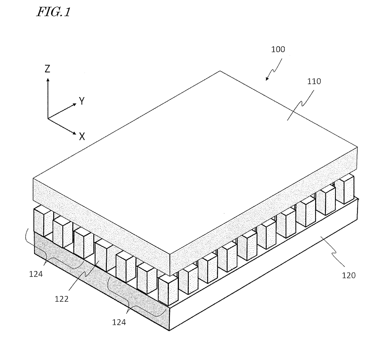
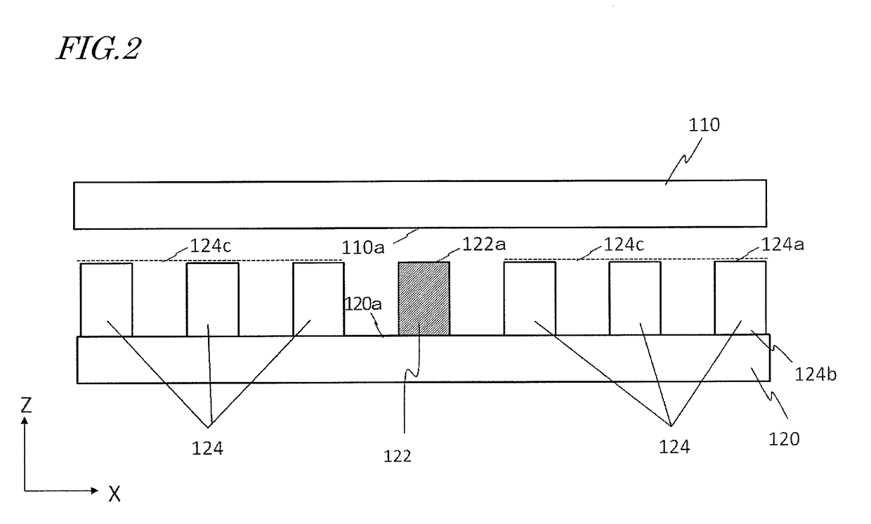
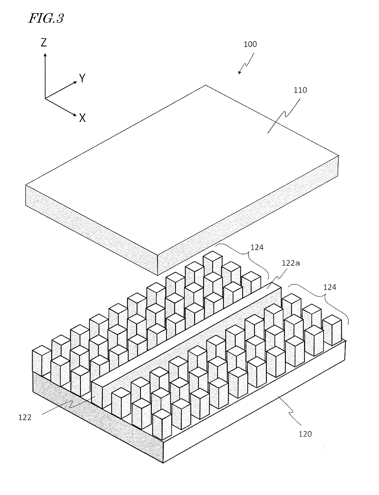
A waveguide device includes: a circuit board having a microstrip line thereon; a microwave IC connected to one end of the microstrip line; a first waffle-iron ridge waveguide; a second waffle-iron ridge waveguide; a first hollow waveguide which is at one end connected to another end of the microstrip line, and at another end connected to a first site of the first waffle-iron ridge waveguide; and a second hollow waveguide which is at one end connected to a second site of the first waffle-iron ridge waveguide, and at another end connected to a first site of the second waffle-iron ridge waveguide.

Description

BACKGROUND1. Technical Field[0001]The present disclosure relates to a waveguide device, and an antenna device including the waveguide device.2. Description of the Related Art[0002]A microwave integrated circuit (IC) is often used as an oscillator circuit for supplying a radio frequency signal to an antenna element in a radar device or a communication device. For example, monolithic microwave integrated circuits (MMIC) are commonly used.[0003]As a transmission line for allowing an electromagnetic wave which is generated from a microwave IC to be transmitted to an antenna element, a hollow waveguide may be used, for example. In a radar device which is disclosed in Patent Document 1, a microwave IC that is mounted on a transmission / reception device substrate is disposed at a position opposing one of the openings of the hollow waveguide. The hollow waveguide and the transmission / reception device substrate are connected via solder balls. The other opening of the hollow waveguide is conne...

Claims


Application Information

Patent Timeline
Patent Type & Authority Applications(United States)
IPC IPC(8): H01Q21/00H01Q21/06
CPCH01Q21/0075H01Q21/064H01P3/123H01Q1/36H01Q1/50H01Q13/0233H01Q21/005H01P5/087H01P5/107
Inventor KAMO, HIROYUKIKIRINO, HIDEKIUSUI, KUMIKO
Owner NIPPON DENSAN CORP
Why Eureka
Try Eureka