Device and method for correcting error estimation of analog-to-digital converter
a technology of error estimation and analog-to-digital converter, which is applied in the field of analog-to-digital converter, can solve the problems of reducing the performance of ti adc, affecting the accuracy of the affecting the accuracy of correction of error estimation, so as to reduce the effective signal duration, the effect of accurate adjustment of feedback error and increased convergence rate of estimation correction
- Summary
- Abstract
- Description
- Claims
- Application Information
AI Technical Summary
Benefits of technology
Problems solved by technology
Method used
Image
Examples
embodiment 1
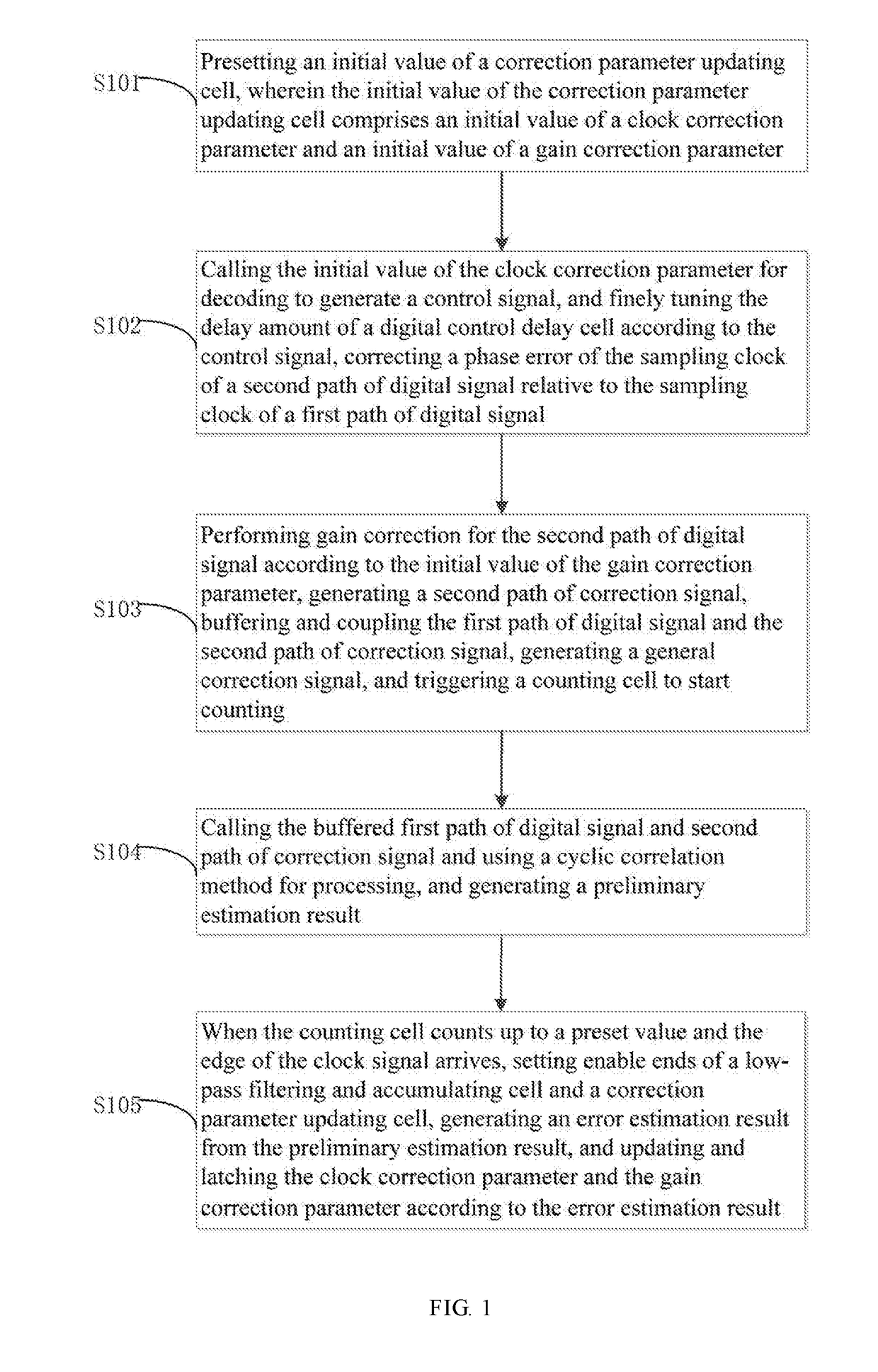
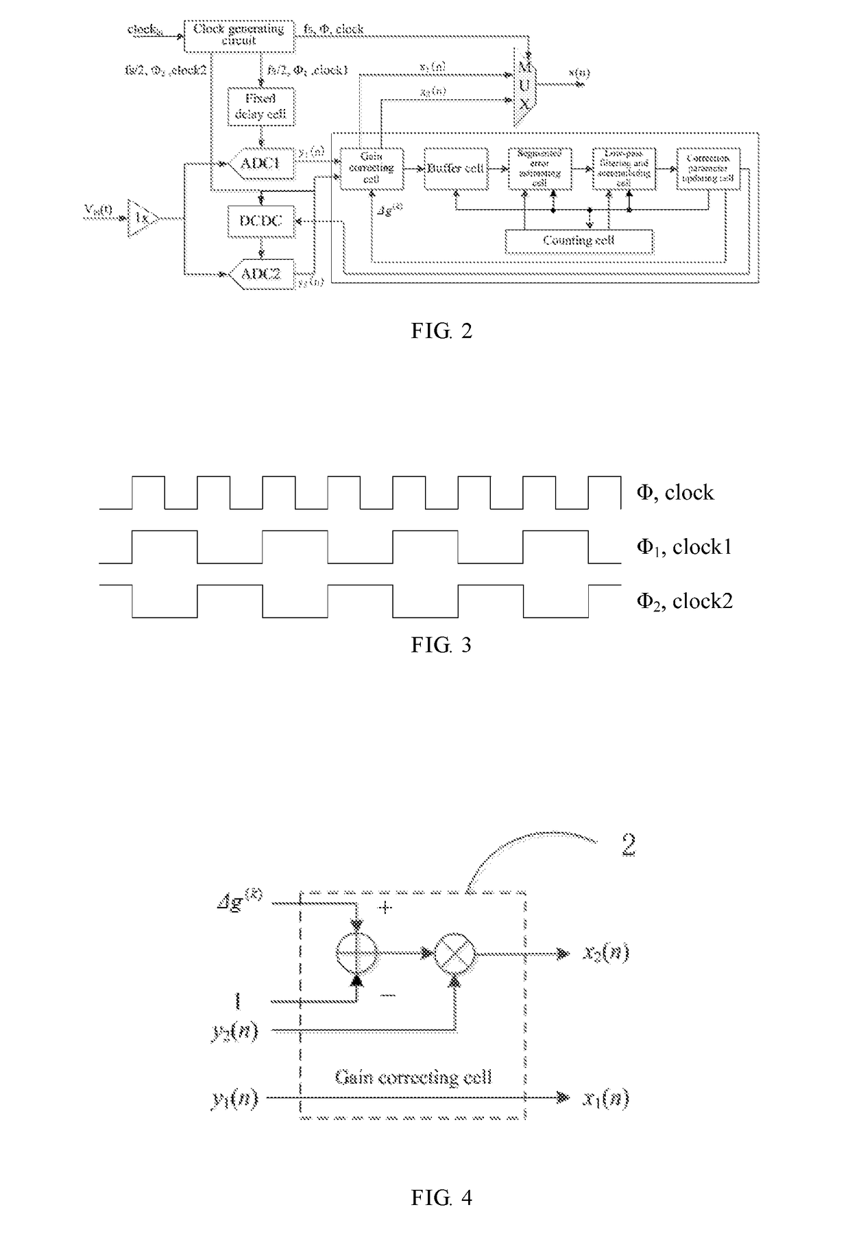
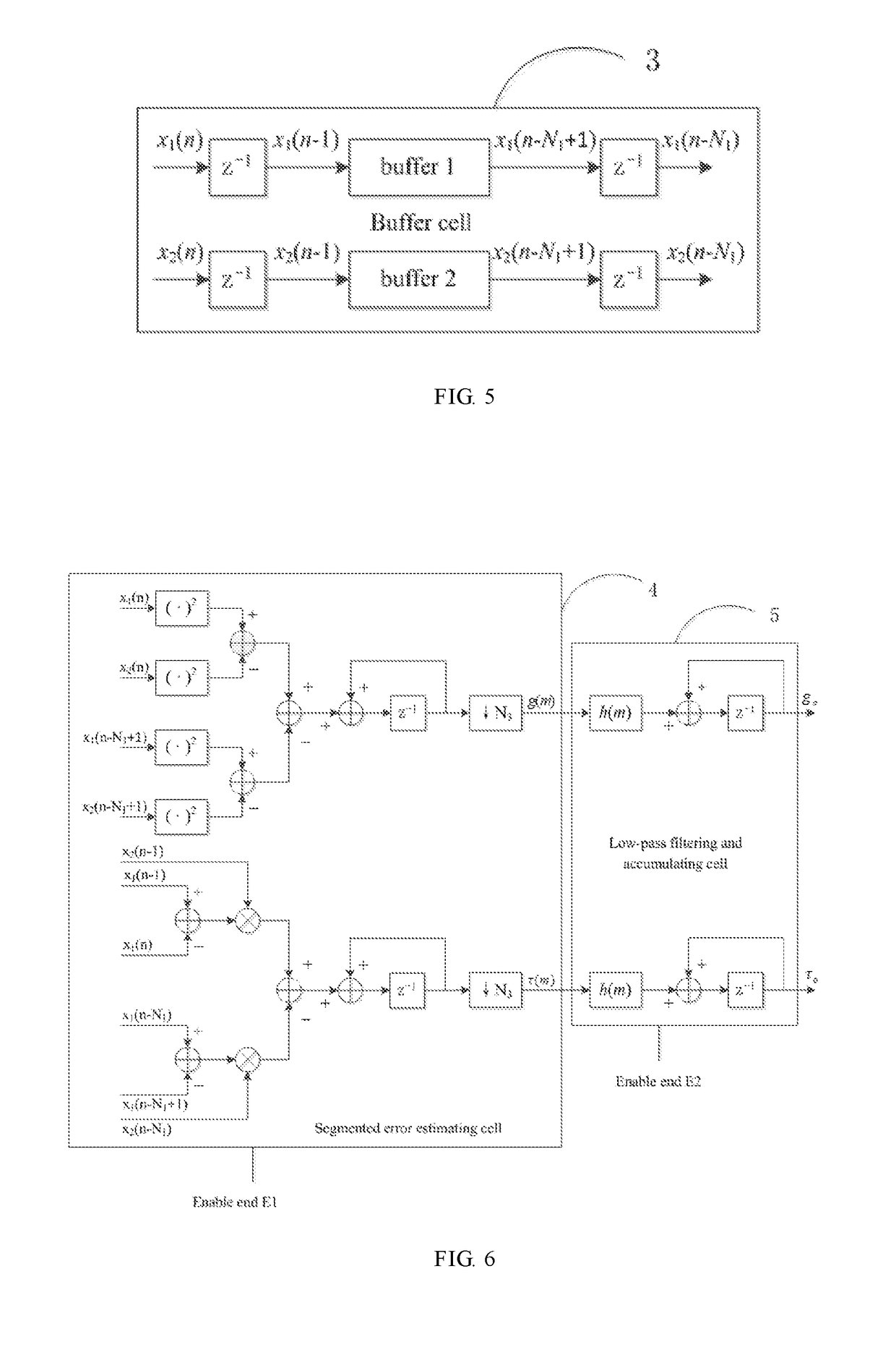
[0070]In the correction of a dual-channel time division multiplexing analog-to-digital converter (TI ADC), a clock signal generator of the TI ADC generates a first path of clock signal and a second path of clock signal according to a clock signal; and the first path of clock signal and the second path of clock signal are clock signals which are the same in cycle and have a phase difference of 180 degrees. The first channel sub-ADC samples and maintains a input signal during the cycle of the first path of clock signal to provide a first path of digital signal as a reference signal; the second channel sub-ADC samples and maintains the input signal during the cycle of the second path of clock signal to provide the second path of digital signal as a signal to be corrected.
[0071]A digital control delay cell (DCDC) is set in the sampling clock path of the second path of digital signal, so that the clock phase can be finely tuned to correct the phase error of the second path of clock signa...
embodiment 2
[0091]A single-channel 250-MHz, dual-channel time-interleaved 500-MHz A / D converter with a sampling rate of 14 bits is used as an example for specific description. When the two channel sub-ADCs sample the input signal in parallel, and between sampling clocks, there is a phase difference of 180 degrees between the first clock signal and the second clock signal and the sampling cycle is 4 ns. The output data of the reference channel ADC is set as y1(n); the output data of the correction channel ADC is set as y2(n). DCDC is a digital control delay cell 10, which is controlled by an 8-bit binary code (0-255), totaling 256 codes. The delay step correspondingly adjusted with a unit code is 60 fs. A DCDC same as that in the clock path of the correction channel ADC is inserted in the clock path of the reference channel ADC, wherein, the control code of the DCDC in the clock path of the reference channel ADC is fixed to 128, and the fixed delay achieved is 7.68 ps; the control code of the DC...
PUM
 Abstract
Description
Claims
Application Information


