Methods of making interconnect substrate having stress modulator and crack inhibiting layer and making flip chip assembly thereof

a technology of stress modulator and crack inhibitor, which is applied in the manufacture of printed circuits, printed circuit aspects, basic electric elements, etc., can solve the problems of complex manufacturing requirements, reduced production efficiency, and significant technical limitations, and achieve the effect of reducing warpage in the bump attachment area and cracking of the bump

Inactive Publication Date: 2018-12-13
BRIDGE SEMICON
View PDF0 Cites 4 Cited by
  • Summary
  • Abstract
  • Description
  • Claims
  • Application Information

AI Technical Summary

Benefits of technology

[0015]The method of making the interconnect substrate according to the present invention have numerous advantages. For instance, providing the interconnect pads for bump attachment over the stress modulator is particularly advantageous as the low CTE of the stress modulator can reduce warpage in the bump attachment area and CTE mismatch between the semiconductor device and the bump attachment area can be reduced so that cracking of the bumps in connection with the interconnect pads and the semiconductor device can be avoided. Disposing the first inhibiting layer on the stress modulator and the molding compound t

Problems solved by technology

While flip chip technology has tremendous advantages over wire bonding, its technical limitations are significant.
For instance, solder bumps are vulnerable to stresses or strains induced by thermal expansion mismatch between the semiconductor chip and the package substrate.
However, drawbacks to this approach include complicated manu

Method used


Image

  • Methods of making interconnect substrate having stress modulator and crack inhibiting layer and making flip chip assembly thereof
  • Methods of making interconnect substrate having stress modulator and crack inhibiting layer and making flip chip assembly thereof
  • Methods of making interconnect substrate having stress modulator and crack inhibiting layer and making flip chip assembly thereof

Examples


embodiment 1

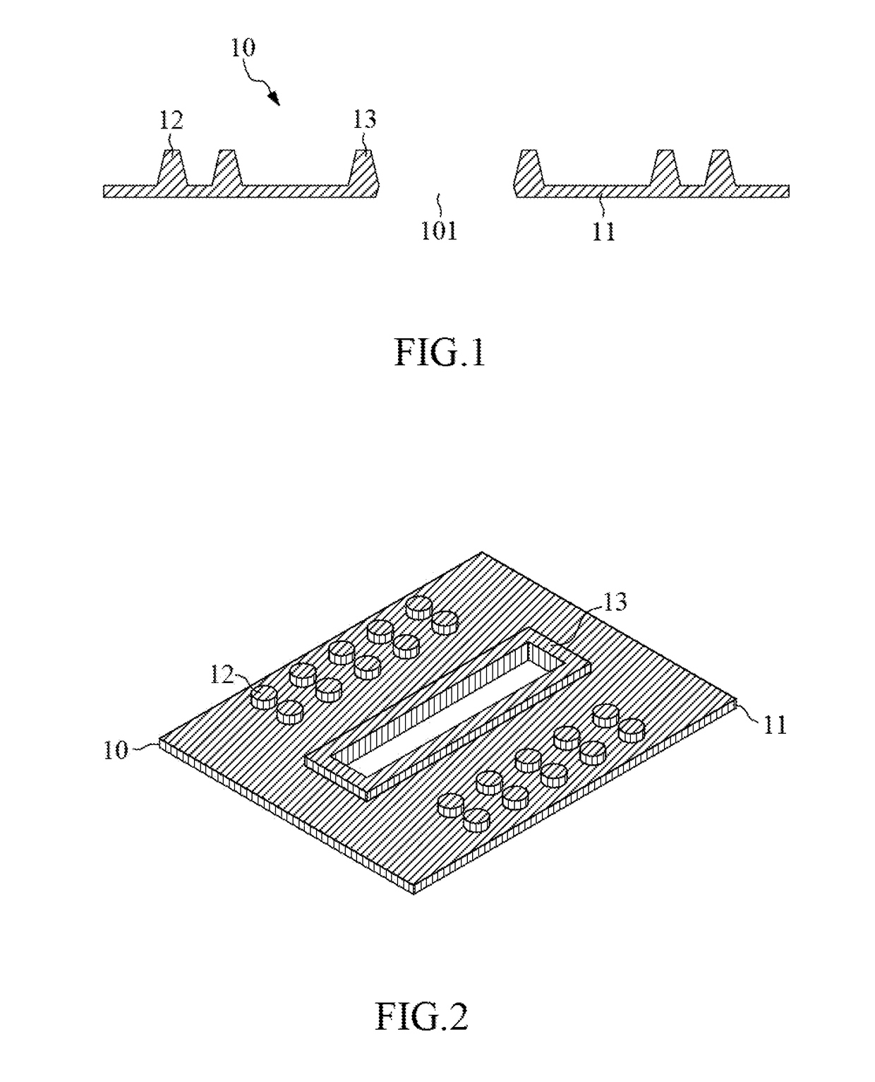
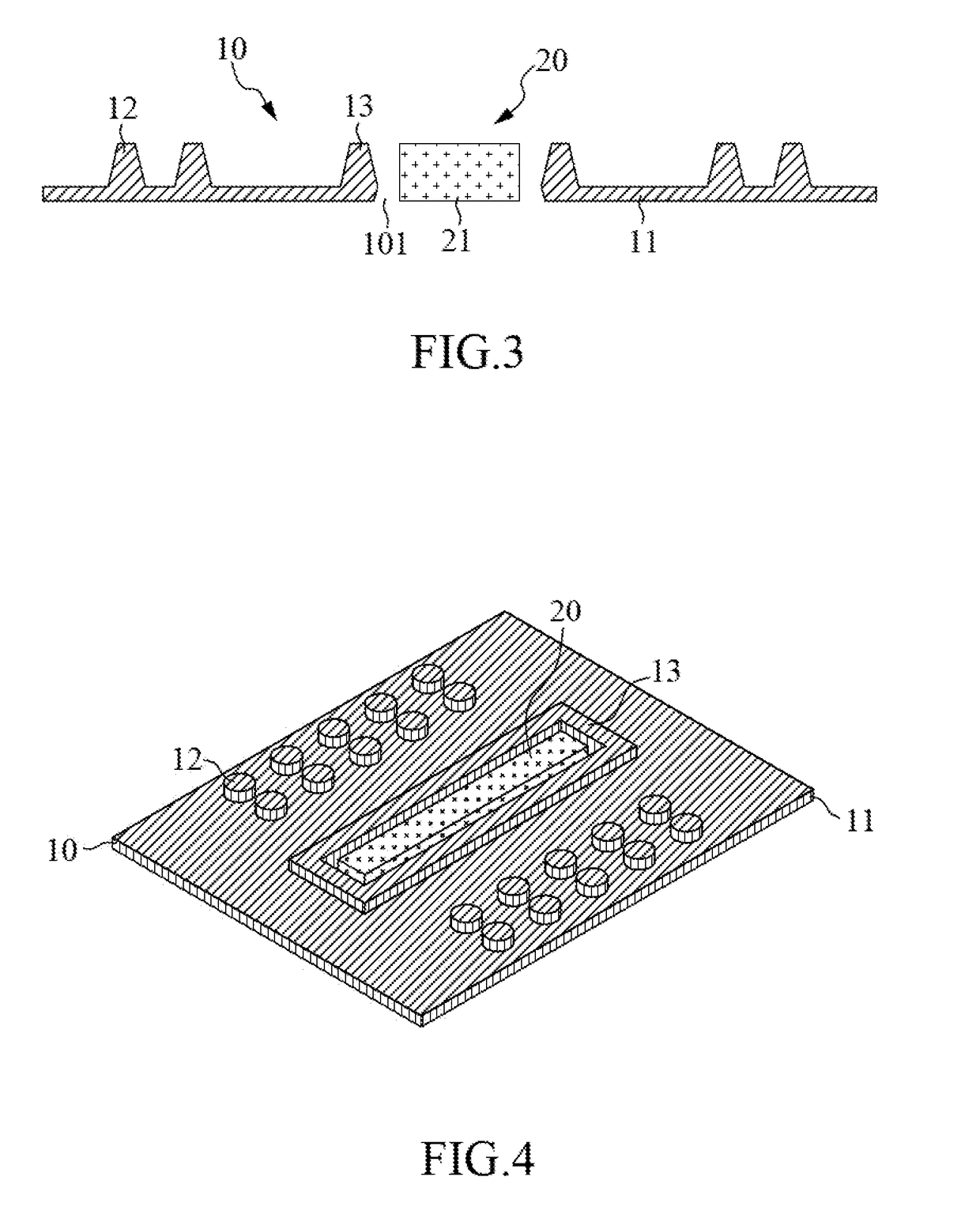
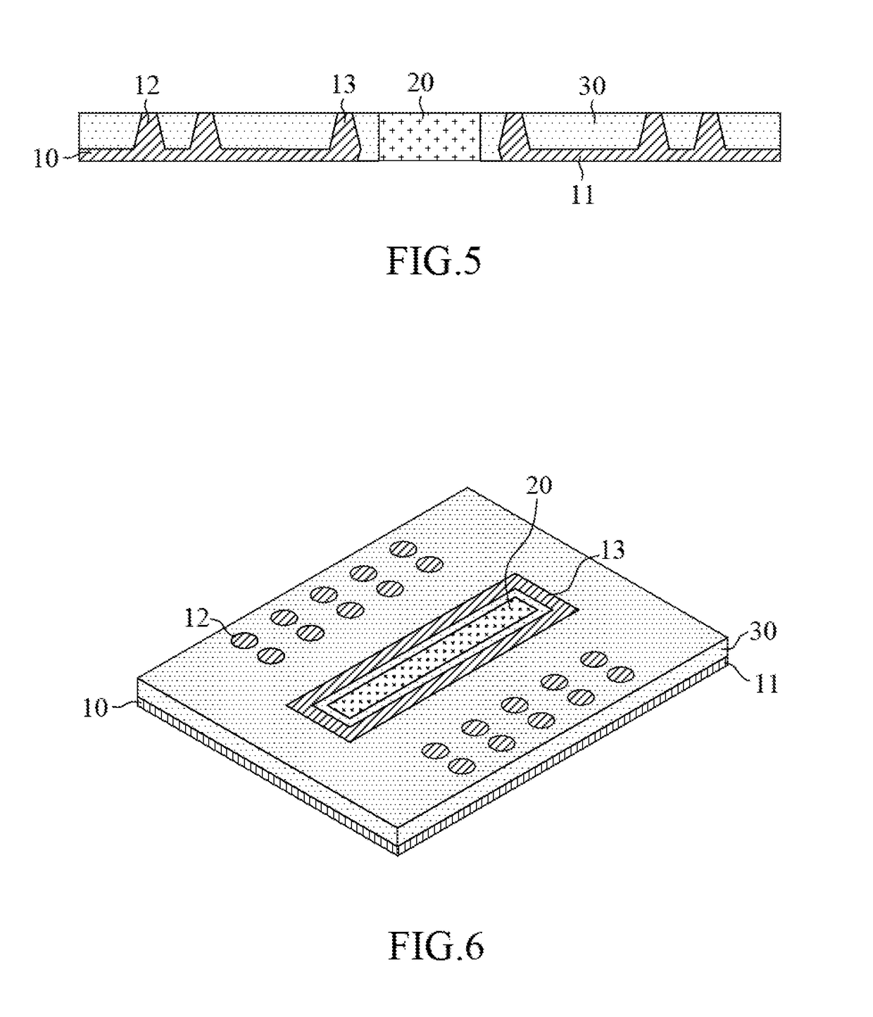
[0048]FIGS. 1-13 are schematic views showing a method of making an interconnect substrate that includes a first array of metal posts, a second array of metal posts, metal rings, a stress modulator, a molding compound, a first crack inhibiting layer and first metal conductors in accordance with the first embodiment of the present invention.

[0049]FIGS. 1 and 2 are cross-sectional and top perspective views, respectively, of a metal plate 10. The metal plate 10 typically is made of copper, aluminum, alloy 42, iron, nickel, silver, gold, combinations thereof, alloys thereof or any other suitable metals. In this embodiment, the metal plate 10 is made of copper and includes a supporting carrier 11, a first array of metal posts 12 and a metal ring 13. The first array of metal posts 12 and the metal ring 13 contact and project from a top side of the supporting carrier 11. The metal ring 13 laterally surrounds a pre-determined location for placement of a stress modulator, and the first array ...

embodiment 2

[0063]FIGS. 17-18 are schematic views showing a method of making an interconnect substrate with a second crack inhibiting layer and second metal conductors in accordance with the second embodiment of the present invention.

[0064]For purposes of brevity, any description in Embodiment 1 above is incorporated herein insofar as the same is applicable, and the same description need not be repeated.

[0065]FIG. 17 is a cross-sectional view of the structure of FIG. 12 further provided with a second crack inhibiting layer 52 and via openings 53 in the second crack inhibiting layer 52. The second crack inhibiting layer 52 covers and contacts the bottom surface of the stress modulator 20 and the bottom surface of the molding compound 30 as well as the bottom sides of the metal posts 14 and the metal ring 15 from below. The via openings 53 extend through the second crack inhibiting layer 52 to expose selected portions of the metal posts 14 and the metal ring 15 from below. In this embodiment, the...

embodiment 3

[0069]FIGS. 20-24 are schematic views showing a method of making an interconnect substrate with primary metal conductors on the molding compound in accordance with the third embodiment of the present invention.

[0070]For purposes of brevity, any description in the Embodiments above is incorporated herein insofar as the same is applicable, and the same description need not be repeated.

[0071]FIG. 20 is a cross-sectional view of the structure of FIG. 5 further provided with primary metal conductors 41 on the molding compound 30. The primary metal conductors 41 contact and extend laterally on the top surface of the molding compound 30 and are electrically connected to the first array of metal posts 12 and the metal ring 13.

[0072]FIG. 21 is a cross-sectional view of the structure with a first crack inhibiting layer 42 and via openings 43. The first crack inhibiting layer 42 covers the top surface of the stress modulator 20 and further extends laterally over interfaces between the stress m...


PUM


Abstract

A method of making an interconnect substrate mainly includes steps of: providing metal posts around a stress modulator, providing a molding compound to bind the stress modulator and the metal posts, providing a crack inhibiting layer on the stress modulator and the molding compound and interfaces between the stress modulator and the molding compound, and depositing metal conductors on the crack inhibiting layer and electrically connected to the metal posts. The metal conductors have interconnect pads superimposed over the stress modulator so that bumps for device connection can be mounted at the area covered by the stress modulator, thereby avoiding cracking of the bumps.

Description

CROSS REFERENCE TO RELATED APPLICATIONS[0001]This application is a continuation-in-part of U.S. application Ser. No. 14 / 846,987 filed Sep. 7, 2015, a continuation-in-part of U.S. application Ser. No. 15 / 080,427 filed Mar. 24, 2016, a continuation-in-part of U.S. application Ser. No. 15 / 605,920 filed May 25, 2017, a continuation-in-part of U.S. application Ser. No. 15 / 642,253 filed Jul. 5, 2017, a continuation-in-part of U.S. application Ser. No. 15 / 881,119 filed Jan. 26, 2018, a continuation-in-part of U.S. application Ser. No. 15 / 908,838 filed Mar. 1, 2018, and a continuation-in-part of U.S. application Ser. No. 15 / 976,307 filed May 10, 2018.[0002]The U.S. application Ser. No. 14 / 846,987 is a continuation-in-part of U.S. application Ser. No. 14 / 621,332 filed Feb. 12, 2015. The U.S. application Ser. No. 15 / 080,427 is a continuation-in-part of U.S. application Ser. No. 14 / 621,332 filed Feb. 12, 2015 and a continuation-in-part of U.S. application Ser. No. 14 / 846,987 filed Sep. 7, 2015...

Claims


Application Information

Patent Timeline
IPC IPC(8): H05K13/00H05K13/04H01L21/56H01L21/48H01L23/498
CPCH05K13/00H05K13/0469H01L21/568H01L21/4857H01L23/49838H01L23/49822H01L23/3121H01L2224/16227H01L2224/18H05K2203/063H05K2203/025H05K2201/0187H05K1/0204H05K13/0486H05K2201/10106H01L23/3677H01L23/49827H01L2224/16225H01L2224/32225H01L2224/73204H01L2224/92125H01L2924/15173H01L2924/1531H01L2924/15311H01L2924/15313H01L2924/3511H01L2924/3512H01L23/562H01L24/16H01L24/32H01L24/73H01L21/486H01L2924/00012H01L2924/00
Inventor LIN, CHARLES W. C.WANG, CHIA-CHUNG
Owner BRIDGE SEMICON
Why Eureka
Try Eureka