

Method of forming semiconductor device
- Summary
- Abstract
- Description
- Claims
- Application Information
AI Technical Summary
Benefits of technology
Problems solved by technology
Method used
Image

Examples
first embodiment
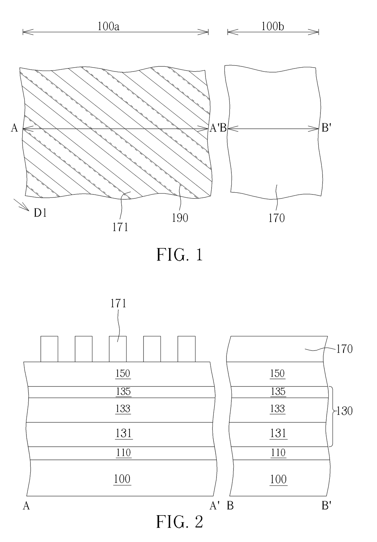
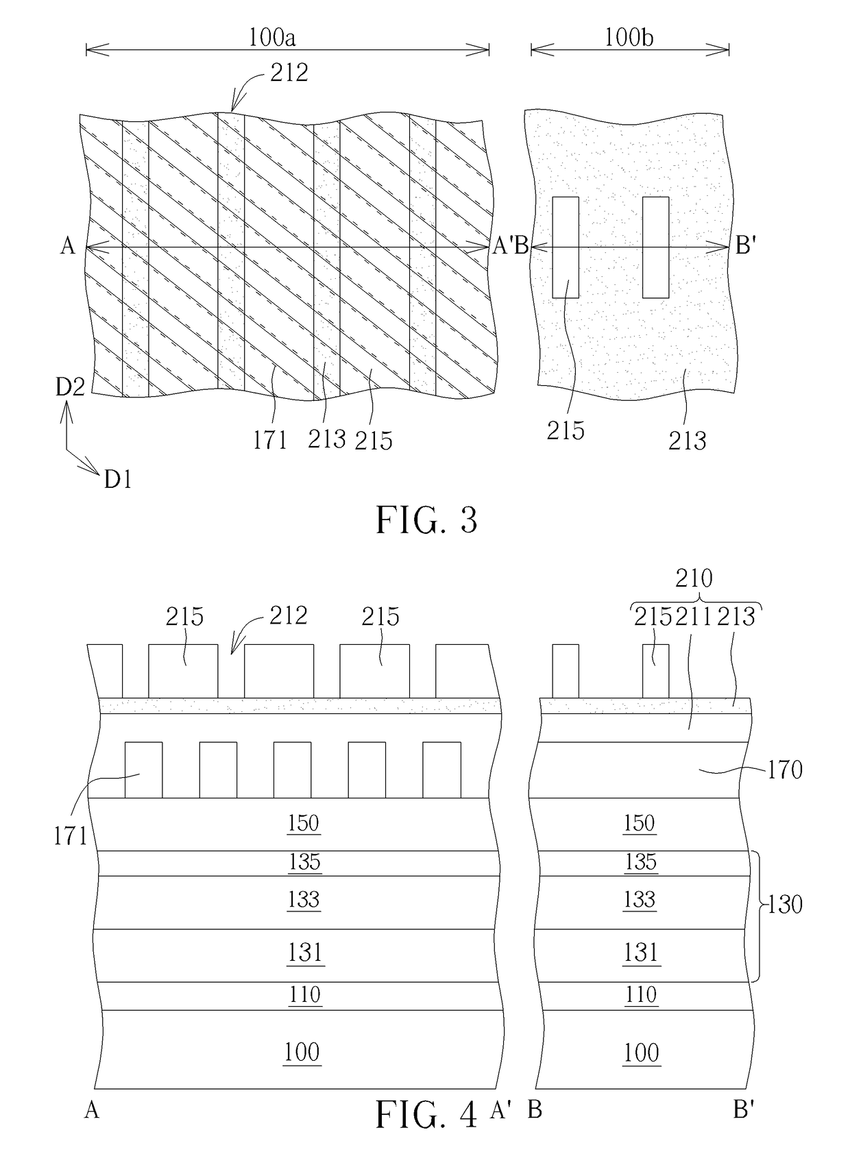
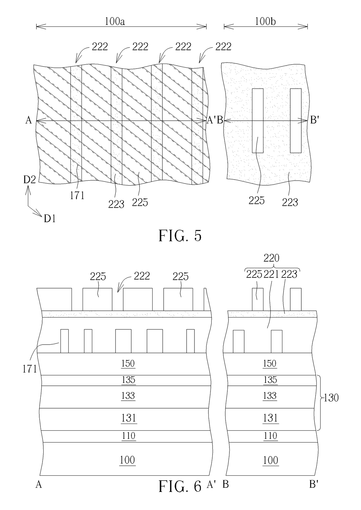
[0024]Please refer to FIG. 1 to FIG. 8, which are schematic diagrams illustrating a forming process of a semiconductor device according to the present invention, wherein FIGS. 1, 3, 5 and 7 respectively show a top view of the semiconductor device during the forming process, and other figures respectively show a cross-sectional view along cross lines A-A′, B-B′ and C-C′ in FIGS. 1, 3, 5 and 7.
[0025]First of all, a substrate layer 100 is provided, and the substrate layer 100 for example includes a semiconductor substrate (not shown in the drawings) like a silicon substrate, a silicon containing substrate or a silicon-on-insulator (SOI) substrate, and / or a dielectric layer (not shown in the drawings), such as including silicon oxide (SiOx), silicon nitride (SiN) or silicon oxynitride (SiON), stacked on the semiconductor substrate, but is not limited thereto. The substrate layer 100 has a first region 100a and a second region 100b, and a target layer 110, a hard mask layer 130 and a mas...
second embodiment
[0044]According to the aforementioned processes, a method of forming a semiconductor device is accomplished. In the present method, the SIT technique and the pattern splitting technique are optionally used to respectively form the mask patterns and the openings which are extended in different directions to cross with each other. That is, the present method may also obtain tiny hard mask patterns and / or target patterns in a more densely layout under a simplified process flow using a reduced number of photo masks.
[0045]Referring to FIGS. 11-13, which are schematic diagrams illustrating a forming process of a semiconductor device according to the third embodiment of the present invention. The formal steps in the present embodiment are similar to those in the second embodiment, and which will not redundantly described herein. The differences between the present embodiment and the aforementioned second embodiment are that, after forming the mask patterns 171a within the first region 100...
third embodiment
[0050]According to the aforementioned processes, a method of forming a semiconductor device is accomplished. In the present method, the SIT technique and the pattern splitting technique are optionally used to form the mask patterns and the openings which are extended in different direction. Also, the mask patterns and the openings may be either across or perpendicular to each other, so as to form tiny hard mask patterns and / or target patterns in a more densely layout under a simplified process flow using a reduced number of photo masks.
[0051]In overall speaking, the method of the present invention utilizes a multiple patterning process, such as the SIT process and the pattern splitting process, to form the mask patterns and the openings respectively in a material layer, such as the hard mask layer and / or the target layer. The mask patterns and the openings are extended along different directions, with those mask patterns and the openings either across with each other or perpendicul...
PUM
 Abstract
Description
Claims
Application Information