Fet with micro-scale device array

Active Publication Date: 2019-01-03
TELEDYNE SCI & IMAGING
View PDF5 Cites 4 Cited by
  • Summary
  • Abstract
  • Description
  • Claims
  • Application Information

AI Technical Summary

Benefits of technology

[0004]A FET employing a micro-scale device array structure is presented, whi

Problems solved by technology

The increased channel temperature limits the power performance (gain, output power, efficiency, linearity) of FET's used as power amplifiers and shortens their lifetime.
However, this approach increases device unit cell size and reduces area power density.
But unit cell size is limited by both gate resistance and phase-delay at a

Method used


Image

  • Fet with micro-scale device array
  • Fet with micro-scale device array
  • Fet with micro-scale device array

Examples


Embodiment Construction

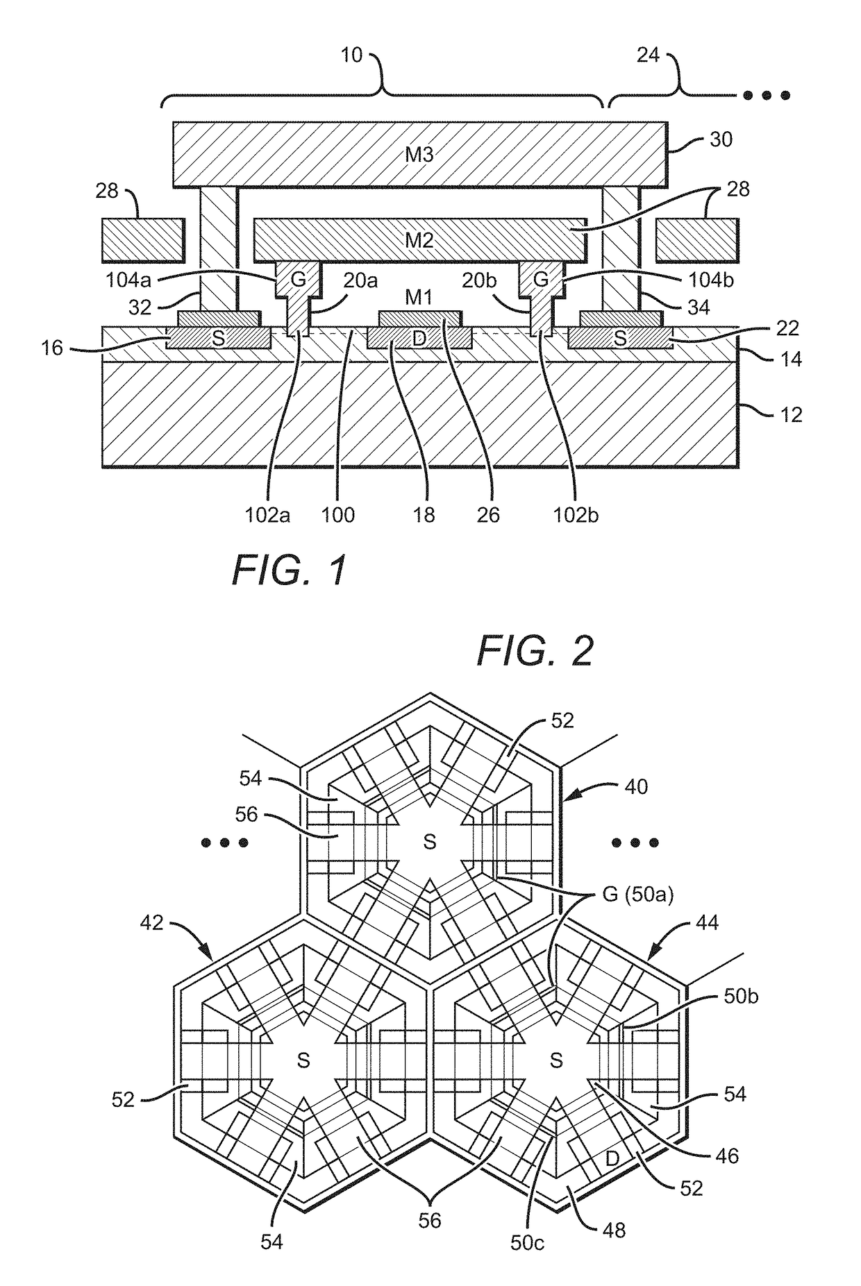
[0018]The present FET employs a micro-scale device array structure, which enables uniform distribution of heat, which is especially beneficial under high power operation. The FET comprises a plurality of interconnected micro-cells. A sectional view of one possible embodiment of a micro-cell in accordance with the invention is shown in FIG. 1. The micro-cell 10 is formed on a substrate 12 on which an epitaxial active channel area 14 has been grown; in practice, a plurality of such micro-cells are uniformly distributed over the active channel area. Each micro-cell comprises a source electrode 16, a drain electrode 18, and at least one gate electrode. Two gate electrodes 20a and 20b are shown in the exemplary embodiment of FIG. 1, which also depicts a source electrode 22 for an adjacent micro-cell 24.

[0019]The micro-cells also comprises a multi-layer interconnection arrangement, wherein a first metal layer 26 (labeled M1) interconnects either the drain or source electrodes (the drain e...


PUM


Abstract

A FET employing a micro-scale device array structure comprises a substrate on which an epitaxial active channel area has been grown, with a plurality of micro-cells uniformly distributed over the active channel area. Each micro-cell comprises a source electrode, a drain electrode, and at least one gate electrode, with a first metal layer interconnecting either the drain or the source electrodes, a second metal layer interconnecting the gate electrodes, and a third metal layer interconnecting the other of the drain or source electrodes. Each micro-cell preferably comprises a source or drain electrode at the center of the micro-cell, with the corresponding drain or source electrode surrounding the center electrode. The number and width of the gate electrodes in each micro-cell may be selected to achieve a desired power density and/or heat distribution, and/or to minimize the FET's junction temperature. The FET structure may be used to form, for example, HEMTs or MESFETs.

Description

BACKGROUND OF THE INVENTIONField of the Invention[0001]This invention relates generally to field-effect transistors (FETs), and more particularly to a FET employing a micro-scale device array structure which enables uniform distribution of heat generated under high power operation.Description of the Related Art[0002]In conventional FETs with long parallel gate fingers, “self-heating” that occurs under high power operation increases the device's channel temperature. The increased channel temperature limits the power performance (gain, output power, efficiency, linearity) of FET's used as power amplifiers and shortens their lifetime.[0003]For such FETs, the junction temperature (Tj) peaks at the drain end of the gate, where the electric field is the highest. The Tj increases with gate width due to increased thermal resistance. To reduce Tj, gate-to-gate pitch can be increased to reduce thermal cross-talk between adjacent gates in the multi-finger devices. However, this approach increa...

Claims


Application Information

Patent Timeline
IPC IPC(8): H01L29/06H01L29/778H01L29/20H01L29/423
CPCH01L29/41758H01L29/4238H01L29/0696H01L23/522H01L29/2003H01L29/20H01L29/4236H01L29/778H01L29/41766H01L29/7786H01L29/812H01L29/24H01L23/528
Inventor SHINOHARA, KEISUKEURTEAGA, MIGUELKING, CASEYBHUNIA, AVIJITCHEN, YA-CHI
Owner TELEDYNE SCI & IMAGING
Why Eureka
Try Eureka