Uniformly encapsulated nanoparticles and uses thereof

a technology of uniform encapsulation and nanoparticles, applied in the field of composite particles, can solve the problems of not enabling the long-term performance required for display or lighting devices, ineffective protection of said surface, and not enabling a long-term stability in time and temperatur

Active Publication Date: 2019-02-07
NEXDOT
View PDF0 Cites 12 Cited by
  • Summary
  • Abstract
  • Description
  • Claims
  • Application Information

AI Technical Summary

Benefits of technology

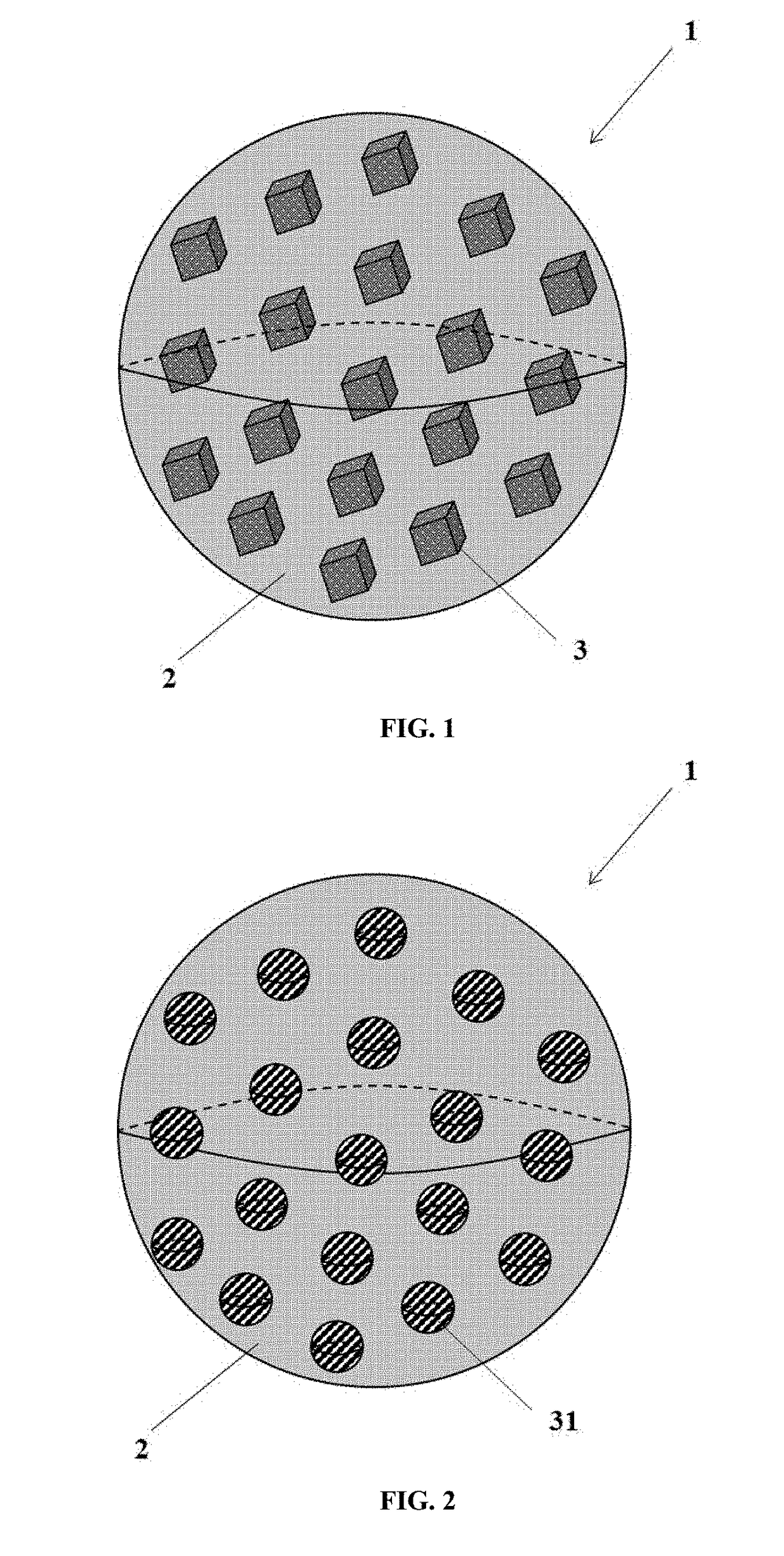
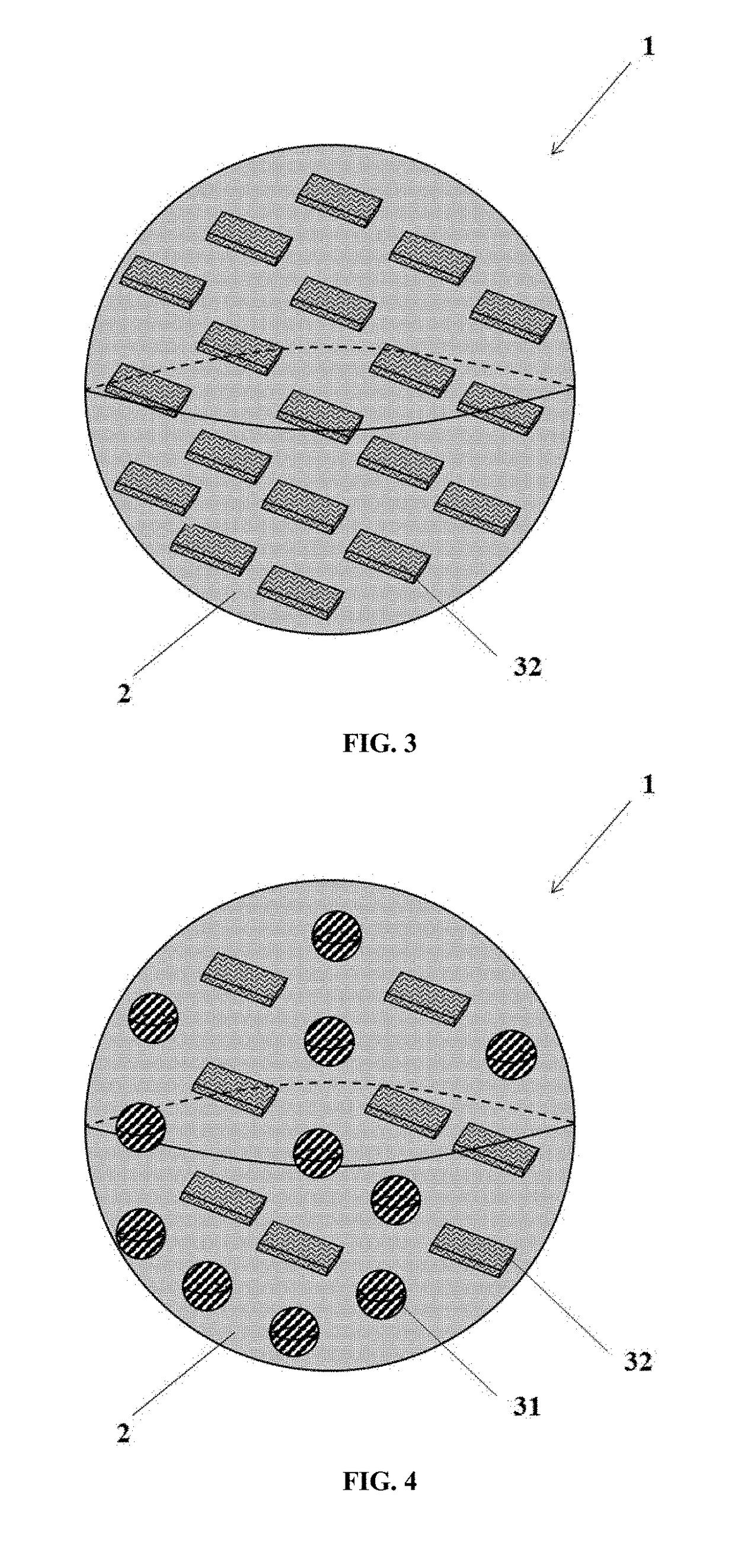
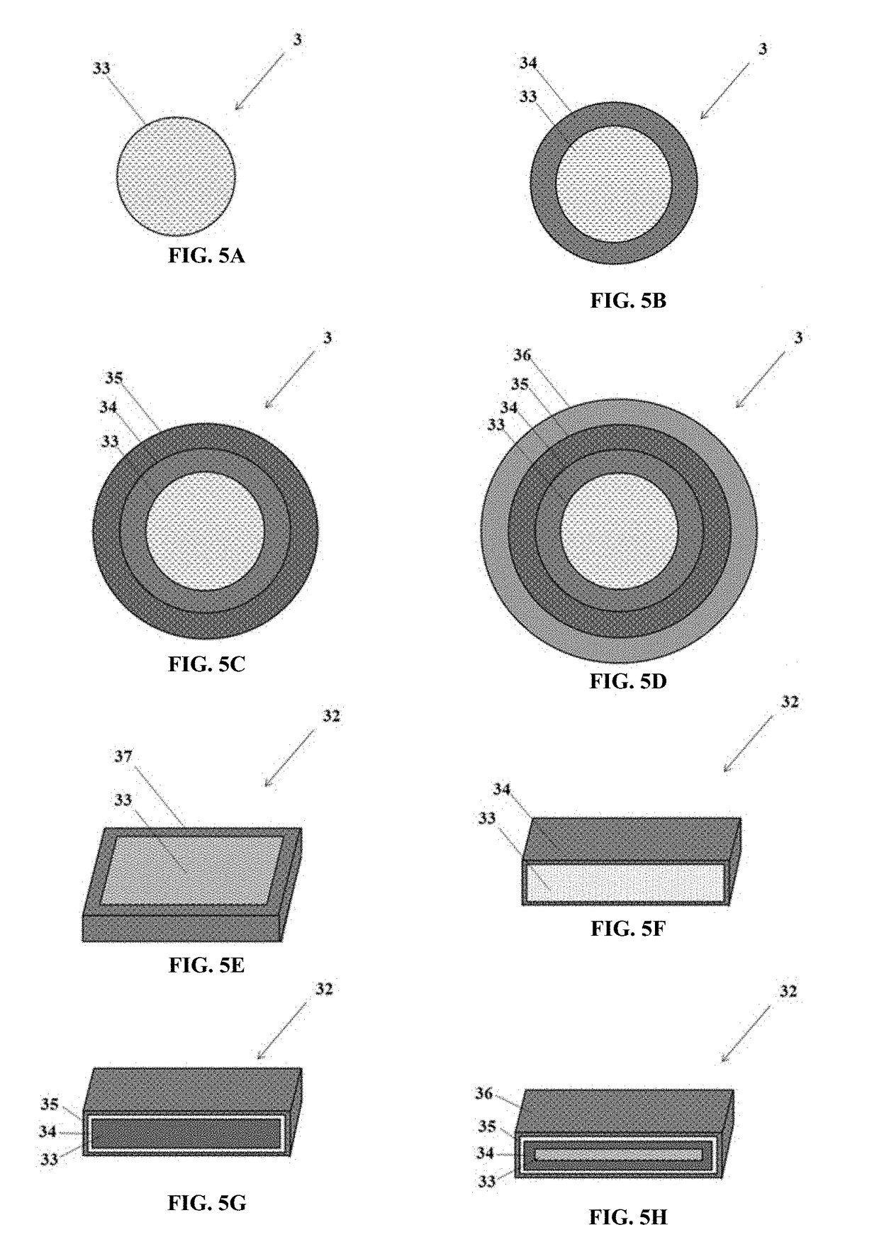
[0015]The invention relates to a composite particle comprising a plurality of nanoparticles encapsulated in an inorganic material, wherein the plurality of nanoparticles is uniformly dispersed in said inorganic material. In one embodiment, each nanoparticle of the plurality of nanoparticles is spaced from its adjacent nanoparticle by an average minimal distance. In one embodiment, the average minimal distance is at least 2 nm. The invention relates to a composite particle comprising a plurality of nanoparticles encapsulated in an inorganic material, wherein the inorganic material is a thermally conductive material. In one embodiment, the inorganic material has a thermal conductivity at standard conditions ranging from 0.1 to 450 W / (m·K). The invention relates to a composite particle comprising a plurality of nanoparticles encapsulated in an inorganic material, wherein the composite particle is impermeable to molecular species, gas or liquid. In one embodiment, the composite particle has an intrinsic permeability to fluids less or equal to 10-11 cm2. In one embodiment, the inorganic material limits or prevents the diffusion of outer molecular species or fluids (liquid or gas) into said inorganic material. In one embodiment, the nanoparticles are luminescent, preferably the luminescent nanoparticles are semiconductor nanocrystals. In one embodiment, the semiconductor nanocrystals comprise a core comprising a material of formula MxNyEzAw, wherein: M is selected from the group consisting of Zn, Cd, Hg, Cu, Ag, Au, Ni, Pd, Pt, Co, Fe, Ru, Os, Mn, Tc, Re, Cr, Mo, W, V, Nd, Ta, Ti, Zr, Hf, Be, Mg, Ca, Sr, Ba, Al, Ga, In, Tl, Si, Ge, Sn, Pb, As, Sb, Bi, Sc, Y, La, Ce, Pr, Nd, Sm, Eu, Gd, Tb, Dy, Ho, Er, Tm, Yb, Cs or a mixture thereof; N is selected from the group consisting of Zn, Cd, Hg, Cu, Ag, Au, Ni, Pd, Pt, Co, Fe, Ru, Os, Mn, Tc, Re, Cr, Mo, W, V, Nd, Ta, Ti, Zr, Hf, Be, Mg, Ca, Sr, Ba, Al, Ga, In, Tl, Si, Ge, Sn, Pb, As, Sb, Bi, Sc, Y, La, Ce, Pr, Nd, Sm, Eu, Gd, Tb, Dy, Ho, Er, Tm, Yb, Cs or a mixture thereof; E is selected from the group consisting of O, S, Se, Te, C, N, P, As, Sb, F, Cl, Br, I, or a mixture thereof; A is selected from the group consisting of O, S, Se, Te, C, N, P, As, Sb, F, Cl, Br, I, or a mixture thereof; and x, y, z and w are independently a decimal number from 0 to 5; x, y, z and w are not simultaneously equal to 0; x and y are not simultaneously equal to 0; z and w may not be simultaneously equal to 0. In one embodiment, the semiconductor nanocrystals comprise at least one shell comprising a material of formula MxNyEzAw, wherein: M is selected from the group consisting of Zn, Cd, Hg, Cu, Ag, Au, Ni, Pd, Pt, Co, Fe, Ru, Os, Mn, Tc, Re, Cr, Mo, W, V, Nd, Ta, Ti, Zr, Hf, Be, Mg, Ca, Sr, Ba, Al, Ga, In, Tl, Si, Ge, Sn, Pb, As, Sb, Bi, Sc, Y, La, Ce, Pr, Nd, Sm, Eu, Gd, Tb, Dy, Ho, Er, Tm, Yb, Cs or a mixture thereof; N is selected from the group consisting of Zn, Cd, Hg, Cu, Ag, Au, Ni, Pd, Pt, Co, Fe, Ru, Os, Mn, Tc, Re, Cr, Mo, W, V, Nd, Ta, Ti, Zr, Hf, Be, Mg, Ca, Sr, Ba, Al, Ga, In, Tl, Si, Ge, Sn, Pb, As, Sb, Bi, Sc, Y, La, Ce, Pr, Nd, Sm, Eu, Gd, Tb, Dy, Ho, Er, Tm, Yb, Cs or a mixture thereof; E is selected from the group consisting of O, S, Se, Te, C, N, P, As, Sb, F, Cl, Br, I, or a mixture thereof; A is selected from the group consisting of O, S, Se, Te, C, N, P, As, Sb, F, Cl, Br, I, or a mixture thereof; and x, y, z and w are independently a decimal number from 0 to 5; x, y, z and w are not simultaneously equal to 0; x and y are not simultaneously equal to 0; z and w may not be simultaneously equal to 0. In one embodiment, the semiconductor nanocrystals comprise at least one crown comprising a material of formula MxNyEzAw, wherein: M is selected from the group consisting of Zn, Cd, Hg, Cu, Ag, Au, Ni, Pd, Pt, Co, Fe, Ru, Os, Mn, Tc, Re, Cr, Mo, W, V, Nd, Ta, Ti, Zr, Hf, Be, Mg, Ca, Sr, Ba, Al, Ga, In, Tl, Si, Ge, Sn, Pb, As, Sb, Bi, Sc, Y, La, Ce, Pr, Nd, Sm, Eu, Gd, Tb, Dy, Ho, Er, Tm, Yb, Cs or a mixture thereof; N is selected from the group consisting of Zn, Cd, Hg, Cu, Ag, Au, Ni, Pd, Pt, Co, Fe, Ru, Os, Mn, Tc, Re, Cr, Mo, W, V, Nd, Ta, Ti, Zr, Hf, Be, Mg, Ca, Sr, Ba, Al, Ga, In, Tl, Si, Ge, Sn, Pb, As, Sb, Bi, Sc, Y, La, Ce, Pr, Nd, Sm, Eu, Gd, Tb, Dy, Ho, Er, Tm, Yb, Cs or a mixture thereof; E is selected from the group consisting of O, S, Se, Te, C, N, P, As, Sb, F, Cl, Br, I, or a mixture thereof; A is selected from the group consisting of O, S, Se, Te, C, N, P, As, Sb, F, Cl, Br, I, or a mixture thereof; and x, y, z and w are independently a decimal number from 0 to 5; x, y, z and w are not simultaneously equal to 0; x and y are not simultaneously equal to 0; z and w may not be simultaneously equal to 0. In one embodiment, the semiconductor nanocrystals are semiconductor nanoplatelets. In one embodiment, the inorganic material comprises a material including but not limited to: silicon oxide, aluminium oxide, titanium oxide, copper oxide, iron oxide, silver oxide, lead oxide, calcium oxide, magnesium oxide, zinc oxide, tin oxide, beryllium oxide, zirconium oxide, niobium oxide, cerium oxide, iridium oxide, scandium oxide, nickel oxide, sodium oxide, barium oxide, potassium oxide, vanadium oxide, tellurium oxide, manganese oxide, boron oxide, phosphorus oxide, germanium oxide, osmium oxide, rhenium oxide, platinum oxide, arsenic oxide, tantalum oxide, lithium oxide, strontium oxide, yttrium oxide, hafnium oxide, tungsten oxide, molybdenum oxide, chromium oxide, technetium oxide, rhodium oxide, ruthenium oxide, cobalt oxide, palladium oxide, cadmium oxide, mercury oxide, thallium oxide, gallium oxide, indium oxide, bismuth oxide, antimony oxide, polonium oxide, selenium oxide, cesium oxide, lanthanum oxide, praseodymium oxide, neodymium oxide, samarium oxide, europium oxide, terbium oxide, dysprosium oxide, erbium oxide, holmium oxide, thulium oxide, ytterbium oxide, lutetium oxide, gadolinium oxide, mixed oxides, mixed oxides thereof, garnets such as for example Y3Al5O12, Y3Fe2(FeO4)3, Y3Fe5O12, Y4Al2O9, YAlO3, Fe3Al2(SiO4)3, Mg3Al2(SiO4)3, Mn3Al2(SiO4)3, Ca3Fe2(SiO4)3, Ca3Al2(SiO4)3, Ca3Cr2(SiO4)3, Al5Lu3O12, GAL, GaYAG, or a mixture thereof. The invention also relates to a light emitting material comprising a host material and at least one composite particle, wherein said at least one composite particle is dispersed in the host material. In one embodiment, the host material comprises an inorganic material, a polymer such as a co-polymer, a block co-polymer, or a silicone-based polymer, a resin such as an epoxy resin or a mixture thereof. In one embodiment, the host material is a thermal conductor. In one embodiment, the host material has a thermal conductivity at standard conditions of at least 0.1 W / (m·K). In one embodiment, the light emitting material further comprises a plurality of composite particles, wherein the plurality of composite particles are uniformly dispersed in the host material. The invention also relates to a support supporting at least one composite particle or a light emitting material, preferably the support is a LED chip or microsized LED. The invention also relates to an optoelectronic device comprising at least one composite particle or a light emitting material.

Problems solved by technology

However, the ligands commonly used to functionalize the surface of quantum dots do not protect efficiently said surface against reactions with deteriorating species or harmful compounds and thus do not enable the long-term performance required for display or lighting devices.
However, said particles are mesoporous which means that they comprise a porous network of silica that allows access to the quantum dots surface for deteriorating species, like water and oxygen, or other harmful compounds.
The protection of said surface is thus ineffective and does not enable a long-term stability in time and temperature.
However, said PbSe quantum dots are aggregated in the silica particles, resulting in a decrease of the photoluminescence quantum yield.
Thus, the aggregation of multiple nanoparticles in a unique particle due to encapsulation results in a dramatic decrease of the property of said nanoparticles.
In the case of luminescent nanoparticles, this results in a decrease of the photoluminescence quantum yield.
However, the resulting particles are not well defined and are aggregated, resulting in a silica matrix-like material comprising quantum dots.
Said material will not allow for a good dispersion in a host material in view of an application as a sub-pixel.

Method used


Image

  • Uniformly encapsulated nanoparticles and uses thereof
  • Uniformly encapsulated nanoparticles and uses thereof
  • Uniformly encapsulated nanoparticles and uses thereof

Examples


example 1

Nanoparticles Preparation

[1796]Nanoparticles used in the examples herein were prepared according to methods of the art (Lhuillier E. et al., Acc. Chem. Res., 2015, 48 (1), pp 22-30; Pedetti S. et al., J. Am. Chem. Soc., 2014, 136 (46), pp 16430-16438; Ithurria S. et al., J. Am. Chem. Soc., 2008, 130, 16504-16505; Nasilowski M. et al., Chem. Rev. 2016, 116, 10934-10982).

[1797]Nanoparticles used in the examples herein were selected in the group comprising CdSe / CdZnS, CdSe, CdS, CdTe, CdSe / CdS, CdSe / ZnS, CdSe / CdZnS, CdS / ZnS, CdS / CdZnS, CdTe / ZnS, CdTe / CdZnS, CdSeS / ZnS, CdSeS / CdS, CdSeS / CdZnS, CuInS2 / ZnS, CuInSe2 / ZnS, InP / CdS, InP / ZnS, InZnP / ZnS, InP / ZnSeS, InP / ZnSe, InP / CdZnS, CdSe / CdZnS / ZnS, CdSe / ZnS / CdZnS, CdSe / CdS / ZnS, CdSe / CdS / CdZnS, CdSe / ZnSe / ZnS, CdSeS / CdS / ZnS, CdSeS / CdS / CdZnS, CdSeS / CdZnS / ZnS, CdSeS / ZnSe / ZnS, CdSeS / ZnSe / CdZnS, CdSeS / ZnS / CdZnS, CdSe / ZnS / CdS, CdSeS / ZnS / CdS, CdSe / ZnSe / CdZnS, InP / ZnSe / ZnS, InP / CdS / ZnSe / ZnS, InP / CdS / ZnS, InP / ZnS / CdS, InP / GaP / ZnS, InP / GaP / ZnSe, InP / CdZ...

example 2

Ligands for Phase Transfer in Basic Aqueous Solution

[1798]100 μL of CdSe / CdZnS nanoplatelets suspended in heptane were mixed with 3-mercaptopropionic acid and heated at 60° C. for several hours. The nanoparticles were then precipitated by centrifugation and redispersed in dimethylformamide. Potassium tert-butoxide were added to the solution before adding ethanol and centrifugate. The final colloidal nanoparticles were redispersed in water.

example 3

Ligands for Phase Transfer in Acidic Aqueous Solution

[1799]100 μL of CdSe / CdZnS nanoplatelets suspended in a basic aqueous solution were mixed with ethanol and centrifugated. A PEG-based polymer was solubilized in water and added to the precipitated nanoplatelets. Acetic acid was dissolved in the colloidal suspension to control the acidic pH.

Example 4: Composite Particles Preparation from a Basic Aqueous Solution—CdSe / CdZnS@SiO2

[1800]100 μL of CdSe / CdZnS nanoplatelets suspended in a basic aqueous solution were mixed with a basic aqueous solution of TEOS at 0.13M previously hydrolyzed for 24 hours, then loaded on a spray-drying set-up. The liquid mixture was sprayed towards a tube furnace heated at a temperature ranging from the boiling point of the solvent to 1000° C. with a nitrogen flow. The composite particles were collected at the surface of a filter.

[1801]FIG. 10 A-B show TEM images of the resulting particles.

[1802]FIG. 11 A shows the N2 adsorption isotherm of the resulting pa...


PUM

PropertyMeasurementUnit
distanceaaaaaaaaaa
diameteraaaaaaaaaa
average minimal distanceaaaaaaaaaa

Abstract

Disclosed is a composite particle including a plurality of nanoparticles encapsulated in an inorganic material, wherein the plurality of nanoparticles is uniformly dispersed in the inorganic material. Also disclosed is relates to a light emitting material, a support supporting at least one composite particle and/or a light emitting material and an optoelectronic device including at least one composite particle and/or a light emitting material.

Description

FIELD OF INVENTION[0001]The present invention relates to composite particles comprising a plurality of nanoparticles encapsulated and uniformly dispersed in an inorganic material. In particular, the present invention relates to fluorescent composite particles.BACKGROUND OF INVENTION[0002]To represent the colors in all their variety, one proceeds typically by additive synthesis of at least three complementary colors, especially red, green and blue. In a chromaticity diagram, the subset of available colors obtained by mixing different proportions of these three colors is formed by the triangle formed by the three coordinates associated with the three colors red, green and blue.[0003]This subset constitutes what is called a gamut. The majority of color display devices operate on this three-color principle: each pixel consists of three sub-pixels, one red, one green and one blue, whose mixture with different intensities can reproduce a colorful impression.[0004]A luminescent or backlit ...

Claims


Application Information

Patent Timeline
Patent Type & Authority Applications(United States)
IPC IPC(8): C09K11/02C09K11/88C09K11/70C09K11/08C09K11/06C09K11/56H01L33/50
CPCC09K11/025C09K11/883C09K11/703C09K11/0883C09K11/06C09K11/565H01L33/502C09K2211/10C09K11/02C09K11/70B82Y20/00
Inventor POUSTHOMIS, MARCD'AMICO, MICHELEKUNTZMANN, ALEXISLIN, YU-PUCAO, EDGAR
Owner NEXDOT
Why Eureka
Try Eureka