This helps you quickly interpret patents by identifying the three key elements:
Problems solved by technology
Method used
Benefits of technology
Benefits of technology
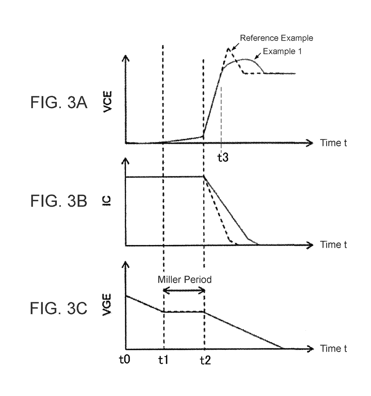
The present invention relates to a semiconductor module with freewheeling diodes and aims to reduce surge voltage at turn-off without increasing switching loss during the Miller period. The invention uses the inductance of the wire between the anode of the freewheeling diode and the reference voltage of the high-side switching device to reduce surge voltage at turn-off time. The first and second wirings are magnetically coupled, and when the high-side switching device turns off, a counter-electromotive force is induced on the first wiring side via the second wiring. This counter-electromotive force is used to reduce the gate drive capability of the high-side switching device, thereby further reducing surge voltage. Overall, this invention allows for a more efficient and reliable semiconductor module with freewheeling diodes.
This in turn results in a problematic increase in switching loss.
However, Patent Document 2 only describes the semiconductor chip itself and does not provide any information related to how to reduce the surge in VCE (surge) in a circuit in which freewheeling diodes are connected in anti-parallel.
However, the technology disclosed in Patent Document 3 is focused on reducing the turn-on current of the low-side semiconductor switch, and at turn-off, the counter-electromotive force is generated to increase Vge, which causes the magnitude of the slope -di / dt to increase and thereby results in an increase in VCE (surge).
Method used
Image
Click on the blue label to locate the original text in one second.
Reading with bidirectional positioning of images and text.
Examples
embodiment 1
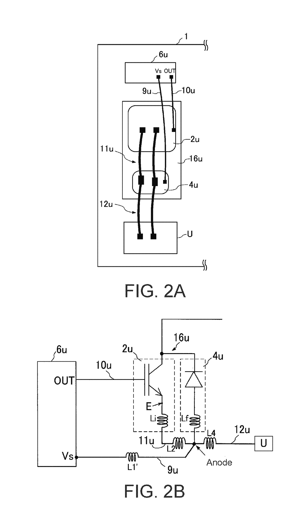
[0051]FIG. 2A illustrates the interior module wiring configuration of the IPM 1 according to Embodiment 1, and FIG. 2B illustrates the circuit configuration of the same. Note that although FIGS. 2A and 2B illustrate the U-phase circuit among the three phases as a representative example, the same configuration can be applied to the other phases as well.
[0052]As illustrated in FIG. 2A, in the IPM 1, an HVIC 6u (6v, 6w) and an external terminal U (V, W) are arranged on an insulating substrate, and between the HVIC 6u (6v, 6w) and the external terminal U (V, W), an IGBT 2u (2v, 2w) and an FWD 4u (4v, 4w) are arranged in that order from the HVIC 6u (6v, 6w) side.
[0053]Moreover, a reference voltage Vs of the HVIC 6u (6v, 6w) is connected to the anode of the FWD 4u (4v, 4w) via a bonding wire 9u (9v, 9w). Furthermore, an output OUT of the HVIC 6u (6v, 6w) is connected to the gate of the IGBT 2u (2v, 2w) via a bonding wire 10u (10v, 10w). The emitter of the IGBT 2u (2v, 2w) is connected to ...
embodiment 2
[0071]Next, Embodiment 2 of the present invention will be described. In the present embodiment, in contrast to the wiring configuration illustrated in FIG. 2A, the bonding wire 9u (9v, 9w) having the inductance L1′ and the bonding wire 11u (11v, 11w) having the inductance L2 are arranged neighboring one another. The resulting magnetic coupling between the inductances L1′ and L2 creates a counter-electromotive force in the inductance L1′ of the bonding wire 9u (9v, 9w) at turn-off of the IGBT 2u (2v, 2w), and this counter-electromotive force is utilized to reduce the gate drive capability of the IGBT 2u (2v, 2w) and to thereby reduce the surge voltage VCE (surge) at turn-off.
[0072]FIG. 6A illustrates the interior module wiring configuration of an IPM 1 according to Embodiment 2 of the present embodiment, and FIG. 6B illustrates the circuit configuration of the same. Note that although FIG. 6A illustrates the U-phase circuit among the three phases as a representative example, the same...
PUM
Abstract
A semiconductor module includes a high-side switching device and a low-side switching device that respectively form an upper arm and a lower arm, freewheeling diodes that are respectively connected to the switching devices in anti-parallel, and a high-side driver circuit and a low-side driver circuit that respectively switch the high-side switching device and the low-side switching device ON and OFF. In the upper arm, an anodeelectrode of the freewheeling diode and a reference voltageelectrode of the high-side driver circuit are directly connected via a first wiring, and the anodeelectrode of the freewheeling diode is connected to a reference voltage electrode of the high-side switching device via a second wiring having an inductance.
Description
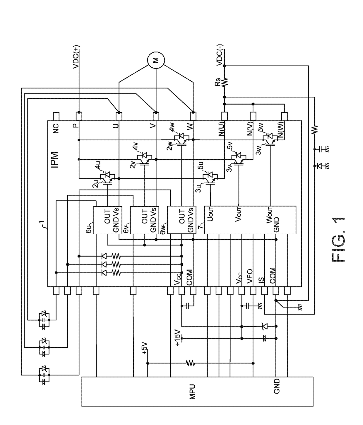
BACKGROUND OF THE INVENTIONTechnical Field[0001]The present invention relates to a semiconductor module which includes high-side semiconductor switching devices and low-side switching devices as well as driver circuits for driving these switching devices, and in which reference voltages of the high-side semiconductor switching devices are connected to reference voltages of the driver circuits.Background Art[0002]Inverters of the type widely used for purposes such as driving motors in consumer and industrial applications typically include semiconductor switching devices such as MOSFETs or IGBTs and driver circuits for driving those semiconductor switching devices. Moreover, intelligent power modules (hereinafter, “IPMs”), which are semiconductor modules in which the semiconductor switching devices and the driver circuits are packaged together to facilitate device miniaturization and inclusion of protection circuits, are also used. Below, an example in which IGBTs are used as the semi...
Claims
Application Information
Patent Timeline
Application Date:The date an application was filed.
Publication Date:The date a patent or application was officially published.
First Publication Date:The earliest publication date of a patent with the same application number.
Issue Date:Publication date of the patent grant document.
PCT Entry Date:The Entry date of PCT National Phase.
Estimated Expiry Date:The statutory expiry date of a patent right according to the Patent Law, and it is the longest term of protection that the patent right can achieve without the termination of the patent right due to other reasons(Term extension factor has been taken into account ).
Invalid Date:Actual expiry date is based on effective date or publication date of legal transaction data of invalid patent.

