Non-volatile memory device and storage device including the same

a technology of non-volatile memory and storage device, applied in the field of non-volatile memory device, can solve problems such as data loss in storage devi

Active Publication Date: 2019-03-28
SAMSUNG ELECTRONICS CO LTD
View PDF12 Cites 12 Cited by
  • Summary
  • Abstract
  • Description
  • Claims
  • Application Information

AI Technical Summary

Benefits of technology

[0005]The inventive concept provides an apparatus and method of eliminating a phase difference between data and a select clock signal of a data multiplexer, and the performing of a data read operation at higher speeds than known heretofore. According to an embodiment of the inventive concept, a combination of a wave pipeline and a serial pipeline are provided to a non-volatile memory device and a storage device including the same.
[0010]According to an embodiment of the inventive concept. a method of eliminating a phase difference in a non-volatile memory device may include storing data, by a First In, First Out (FIFO) memory, transmitted through a data path having a wave pipeline structure based on a plurality of FIFO input clock signals and outputting the stored data based on a plurality of FIFO output clock signals; generating, by a serial pipeline generator, a plurality of serial pipeline driving clock signals that compensate for a phase difference between the stored data output from the FIFO memory and a select clock signal provided to a serializer, a serial pipeline structure including a plurality of serial pipelines, and the serial pipeline structure is connected between the FIFO memory and the serializer; and outputting, by the serializer, data to an input / output pad based on the select clock signal provided to the serializer.

Problems solved by technology

A volatile semiconductor memory device features fast read and write speeds, but data stored therein is lost when an external power supply is interrupted.

Method used


Image

  • Non-volatile memory device and storage device including the same
  • Non-volatile memory device and storage device including the same
  • Non-volatile memory device and storage device including the same

Examples


Embodiment Construction

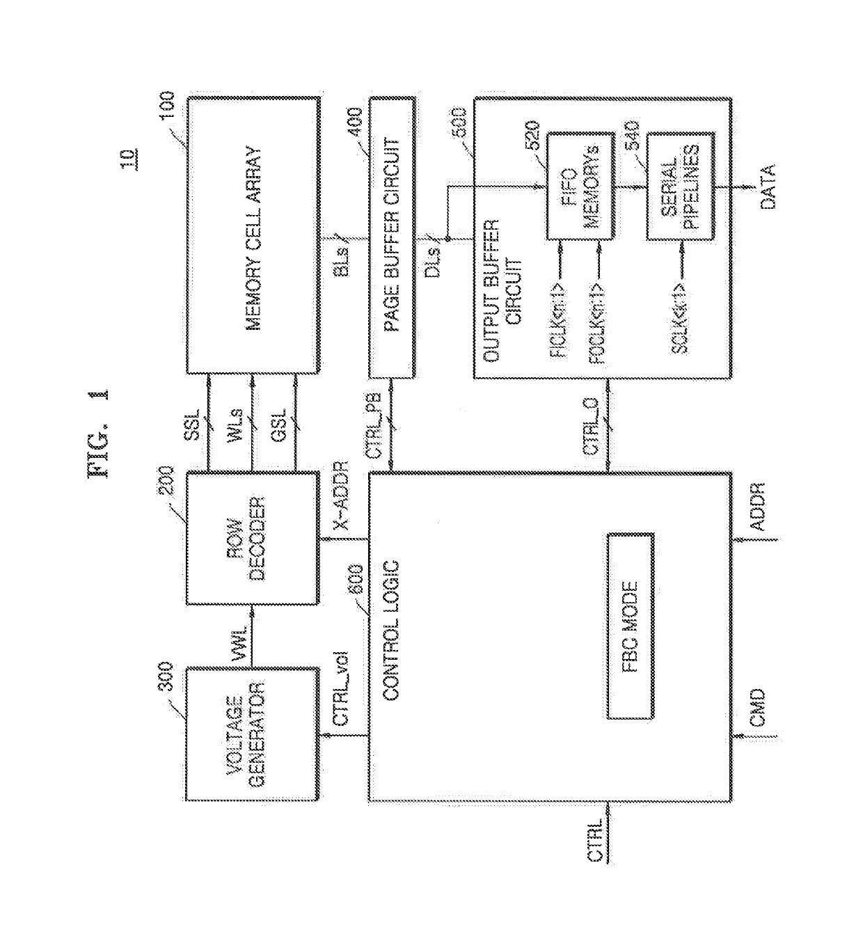
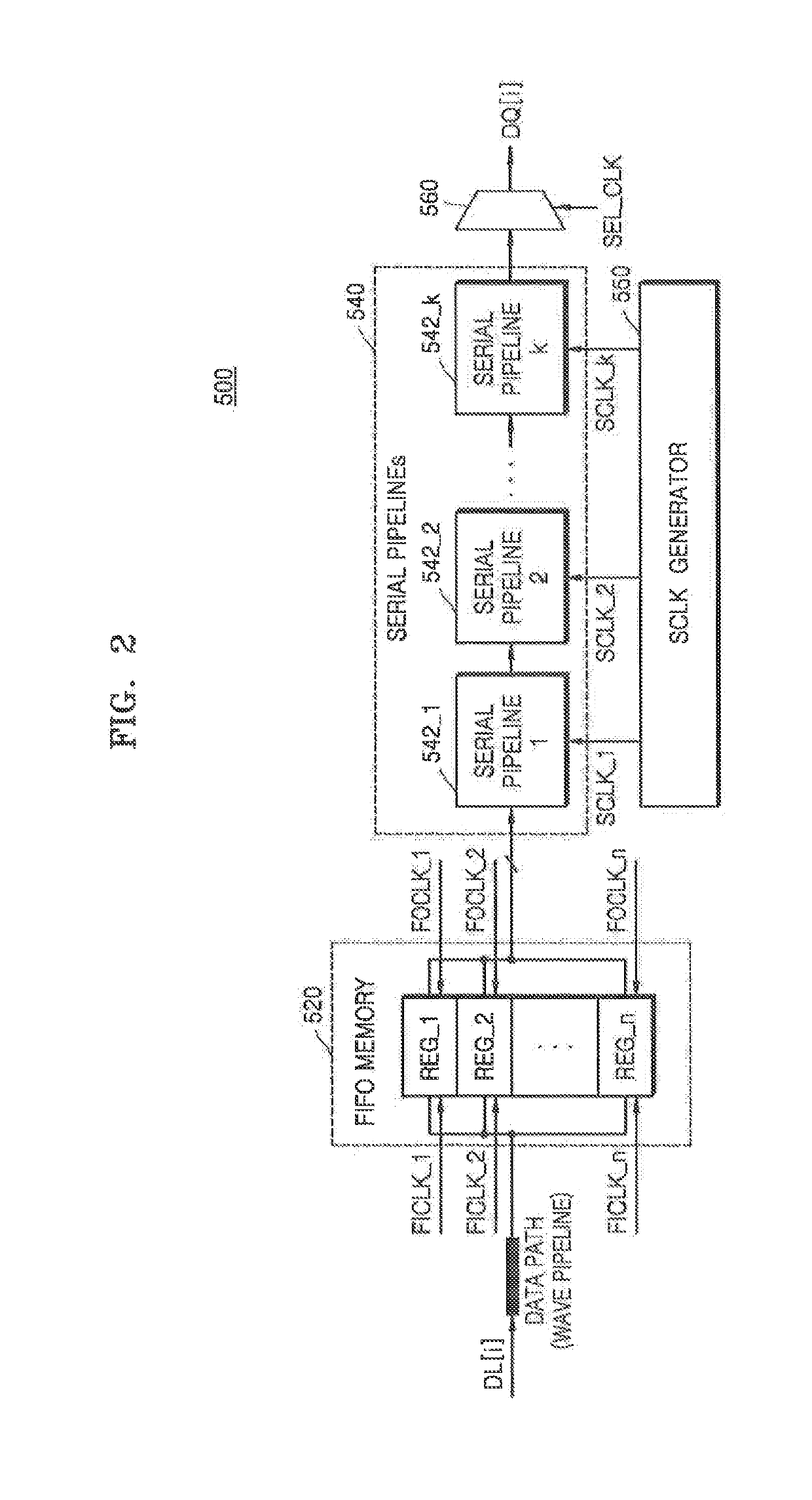
[0033]FIG. 1 is a diagram showing a non-volatile memory device 10 according to an example embodiment of the inventive concept. The non-volatile memory device 10 may include a memory cell array 100, a row decoder 200, a voltage generator 300, a page buffer circuit 400, an output buffer circuit 500, and control logic 600. However, the configuration of the non-volatile memory device 10 is not limited the depiction of FIG. 1, and the non-volatile memory device 10 may further include other components not shown, such as an input buffer circuit and a column decoder.

[0034]Although FIG. 1 shows a non-volatile memory device 10 including one memory cell array 100, embodiments of the inventive concept are not limited thereto. For example, the non-volatile memory device 10 may include a plurality of memory cell arrays 100. The non-volatile memory device 10 of the inventive concept may include, for example, a NAND flash memory, a vertical NAND (VNAND) flash memory, a NOR flash memory, a resistive...


PUM


Abstract

A non-volatile memory device includes a serial pipeline structure connected to an output stage of a First In, First Out (FIFO) memory. The FIFO memory is configured to store data transmitted through a data path having a wave pipeline structure based on a plurality of FIFO input clock signals and output the stored data based on a plurality of FIFO output clock signals. A serializer is configured to output data to an input / output pad based on a select clock signal. The serial pipeline structure is connected between the FIFO memory and the serializer and configured to compensate for a phase difference between the data output from the FIFO memory and the select clock signal.

Description

CROSS-REFERENCE TO RELATED APPLICATION[0001]This application claims the benefit of priority from Korean Patent Application No. 10-2017-0126354, filed on Sep. 28, 2017, in the Korean Intellectual Property Office, the disclosure of which is incorporated by reference herein, in its entirety.TECHNICAL FIELD[0002]The inventive concept relates to a non-volatile memory device, and more particularly, to a non-volatile memory device for sequentially reading out data and a storage device including the same.DISCUSSION OF THE RELATED ART[0003]Semiconductor memory devices may be categorized into volatile memory devices that lose data stored therein when a supply of power is interrupted, and non-volatile memory devices that do not lose data stored therein, even when there is a loss or interruption of power. A volatile semiconductor memory device features fast read and write speeds, but data stored therein is lost when an external power supply is interrupted. On the other hand, a non-volatile semi...

Claims


Application Information

Patent Timeline
Patent Type & Authority Applications(United States)
IPC IPC(8): G11C7/10G11C7/22G11C11/4076G11C11/4096
CPCG11C7/106G11C7/1039G11C7/1087G11C7/22G11C11/4076G11C11/4096G11C7/1051G11C7/1078G11C7/222G11C5/066G11C7/1033G11C7/1066G11C16/26G11C2207/107G06F9/30087G06F9/38
Inventor JANG, DONG-SUYANG, MAN-JAEIHM, JEONG-DONJUNG, GO-EUNJEONG, BYUNG-HOONCHOI, YOUNG-DON
Owner SAMSUNG ELECTRONICS CO LTD
Why Eureka
Try Eureka