Area-Efficient Single-legged SOI MOSFET structure immune to single-event-effects and bipolar latch-up

Active Publication Date: 2019-03-28
TARAKJI AHMAD HOUSSAM
View PDF0 Cites 3 Cited by
  • Summary
  • Abstract
  • Description
  • Claims
  • Application Information

AI Technical Summary

Benefits of technology

[0008]The invention that is claimed provides a new SOI MOS device architecture that further alleviates the effects from this Bipolar latch-up and with a more or a fully area-efficient design that does not reduce or can reduce least the “effective” peripheral Width of the SOI-MOS field-effect Transistors. Its structure is based on trapping the impact-ionization current in a band-engineered highly doped Pocket that junctions the Source on one side while it interfaces the device Body on its other side along the entire device or (Gate) Width (in similarity to the device design of U.S. Pat. No. 9,741,857 B2). This Pocket has same dopant type as in device Body. It traps and diverts the impact-ionization current directly to the Source (instead of diverting it to BTS as in the MOS device structure

Problems solved by technology

This design can still effectively divert impact-ionization current away from the later

Method used


Image

  • Area-Efficient Single-legged SOI MOSFET structure immune to single-event-effects and bipolar latch-up
  • Area-Efficient Single-legged SOI MOSFET structure immune to single-event-effects and bipolar latch-up
  • Area-Efficient Single-legged SOI MOSFET structure immune to single-event-effects and bipolar latch-up

Examples


Embodiment Construction

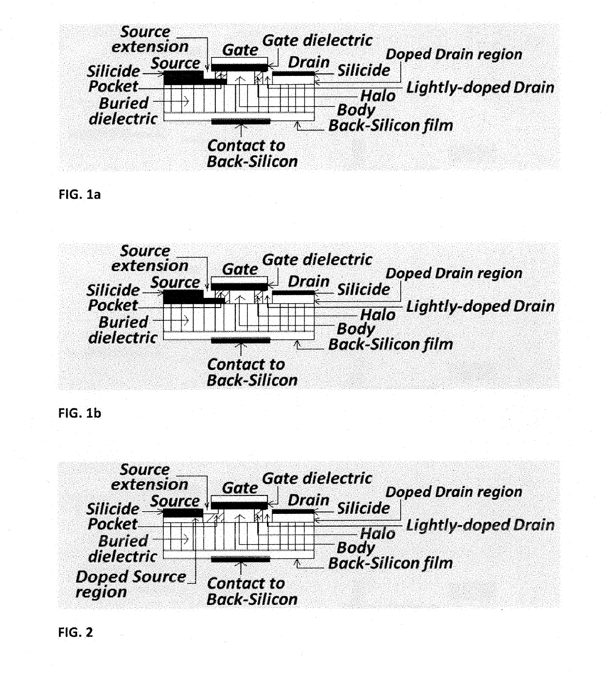
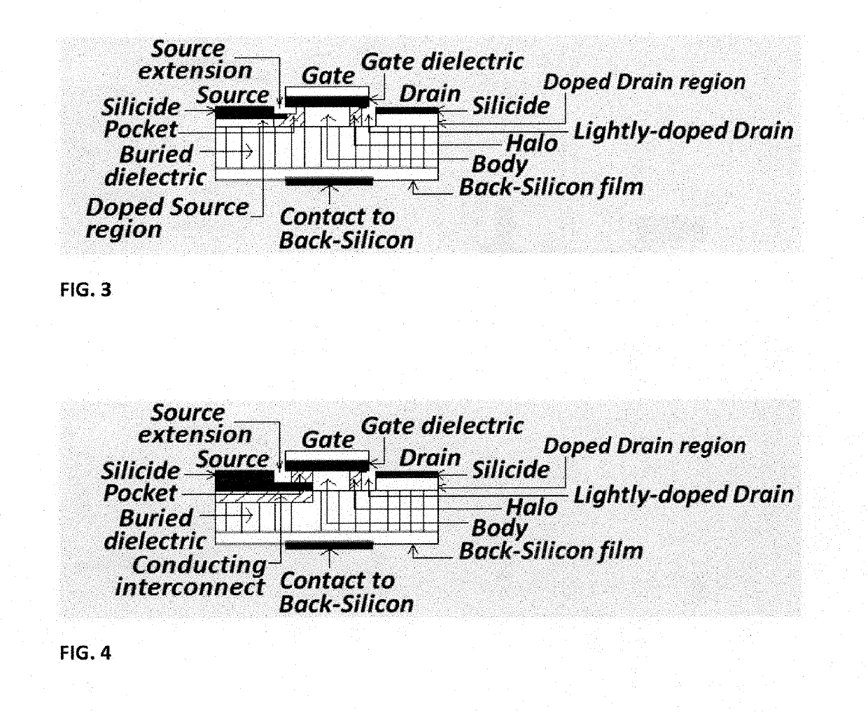
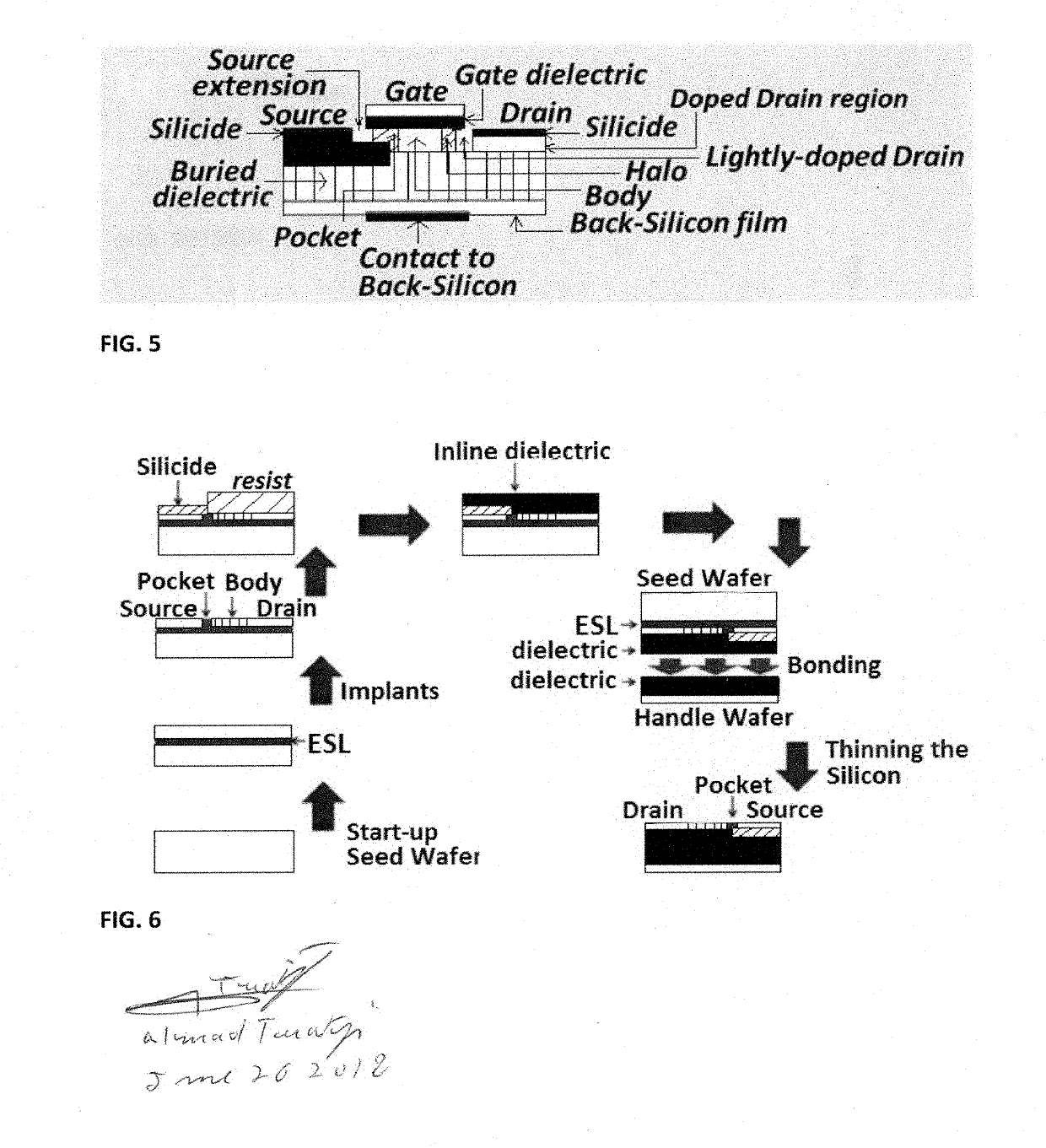
[0016]The new device architecture for SOI MOSFET traps the impact-ionization current in a band-engineered highly doped Pocket that extends in the active Silicon underneath the Gate along the entire device Width and routes this impact-ionization current to the Source-diffusion region through a highly electrically conductive path that contains a Silicide formation that solders this Pocket to the Source. This prevents the impact-ionization current from diffusing through the lateral Body-to-Source barrier and lowering it further. The Silicide in Source region can either consume the entire thickness of active Silicon or only the top portion of it. It may also extend laterally into the highly doped Pocket under the Gate. Square or trenched interconnects may also contact the Silicide to further increase the electric conductance between the device Body under the Gate and the Source. The lightly-doped Drain region helps to suppress the injection of Hot-electrons into the Gate. (Lightly doped...


PUM


Abstract

New device structure for single-legged Silicon-On-Insulator Metal-Oxide-Semiconductor (SOI MOS) transistor is presented. This new structure imposes a hard barrier for an Impact-Ionization current and for transients due to Single-Event-Effects (SEE's) in Body to laterally conduct (or diffuse) to the Source through the Body/Source junction. It forces these currents to conduct instead to the Source through an alternate path made of highly conductive Silicide. This alternate path effectively suppresses the latch-up of the built-in parasitic Bipolar structure without necessitating the incorporation of Body-Tied-Source (BTS) implant into the device structure that increases the total device periphery without correspondingly scaling its device current.

Description

BACKGROUND OF THE INVENTION[0001]There are two primary approaches to the design of large-periphery Metal-Oxide-Semiconductor (MOS) Transistors; one relies on cascading (or arraying) column of multi-Legs (or multi-Fingers) Gates in parallel to enable delivering the required high output current. The other utilizes one single-legged device having sufficiently large Gate width that enables it to deliver same or similar amount of output current. Major advantage of the former approach is that it ensures a desired “Square-like” footprint for any particular large-periphery Transistor Layout. This provides more ease and flexibility in designing and laying-out such Large-periphery Transistors in any given Integrated-Circuit (IC). It can also reduce the device Gate Resistance, and hence it can boost the device power-gain and Bandwidth. The drawback can come however from an excessive increase of the Capacitive parasitic's with the increase of number of Legs (due to a corresponding increase from...

Claims


Application Information

Patent Timeline
IPC IPC(8): H01L29/786H01L27/12H01L29/45H01L29/06
CPCH01L29/78618H01L27/1203H01L29/458H01L29/0607H01L29/78612H01L29/78624
Inventor TARAKJI, AHMAD HOUSSAM
Owner TARAKJI AHMAD HOUSSAM
Why Eureka
Try Eureka