Digital microfluidic devices including dual substrates with thin-film transistors and capacitive sensing

a microfluidic device and capacitive sensing technology, applied in static indicating devices, laboratory glassware, instruments, etc., can solve the problems of inability to perform mass parallel assays, reactions, etc., in passive matrix devices, polysilicon fabrication is substantially more expensive than amorphous silicon fabrication, and achieves the effect of simplifying the fabrication of a device and simplifying the data handling associated

Active Publication Date: 2019-04-18
NUCLERA LTD
View PDF9 Cites 24 Cited by
  • Summary
  • Abstract
  • Description
  • Claims
  • Application Information

AI Technical Summary

Benefits of technology

[0007]In some embodiments, a digital microfluidic device will have two areas of different electrode densities, i.e., a high density (a.k.a. “high-res”) area, and a low density (a.k.a. “low-res”) area for the sensor electrode side. Such a design will allow a user to perform particle interrogation (i.e., capacitive sensing) to determine composition or size in one portion of the device, and then simply monitor the location or presence of particles in another portion of the device. Overall, such a configuration simplifies the fabrication of a device while also simplifying the data handling associated with the sensing functions.

Problems solved by technology

While segmented devices are easy to fabricate, the number of electrodes is limited by space and driving constraints.
Accordingly, it is not possible to perform massive parallel assays, reactions, etc. in passive matrix devices.
However, polysilicon fabrication is substantially more expensive than amorphous silicon fabrication, i.e., the type used in mass-produced active matrix TFTs for the LCD display industry.
Polysilicon fabrication processes are more expensive because there are unique handling and fabrication steps for working with polysilicon.
There are also fewer facilities worldwide that are configured to fabricate devices from polysilicon.
While poly-Si fabrication techniques allow implementation of complex AM-EWoD devices, the costs of poly-Si device production, combined with a global shortage of suitable fabrication facilities, has prevented the AM-EWoD technology from becoming widely available.

Method used


Image

  • Digital microfluidic devices including dual substrates with thin-film transistors and capacitive sensing
  • Digital microfluidic devices including dual substrates with thin-film transistors and capacitive sensing
  • Digital microfluidic devices including dual substrates with thin-film transistors and capacitive sensing

Examples


Embodiment Construction

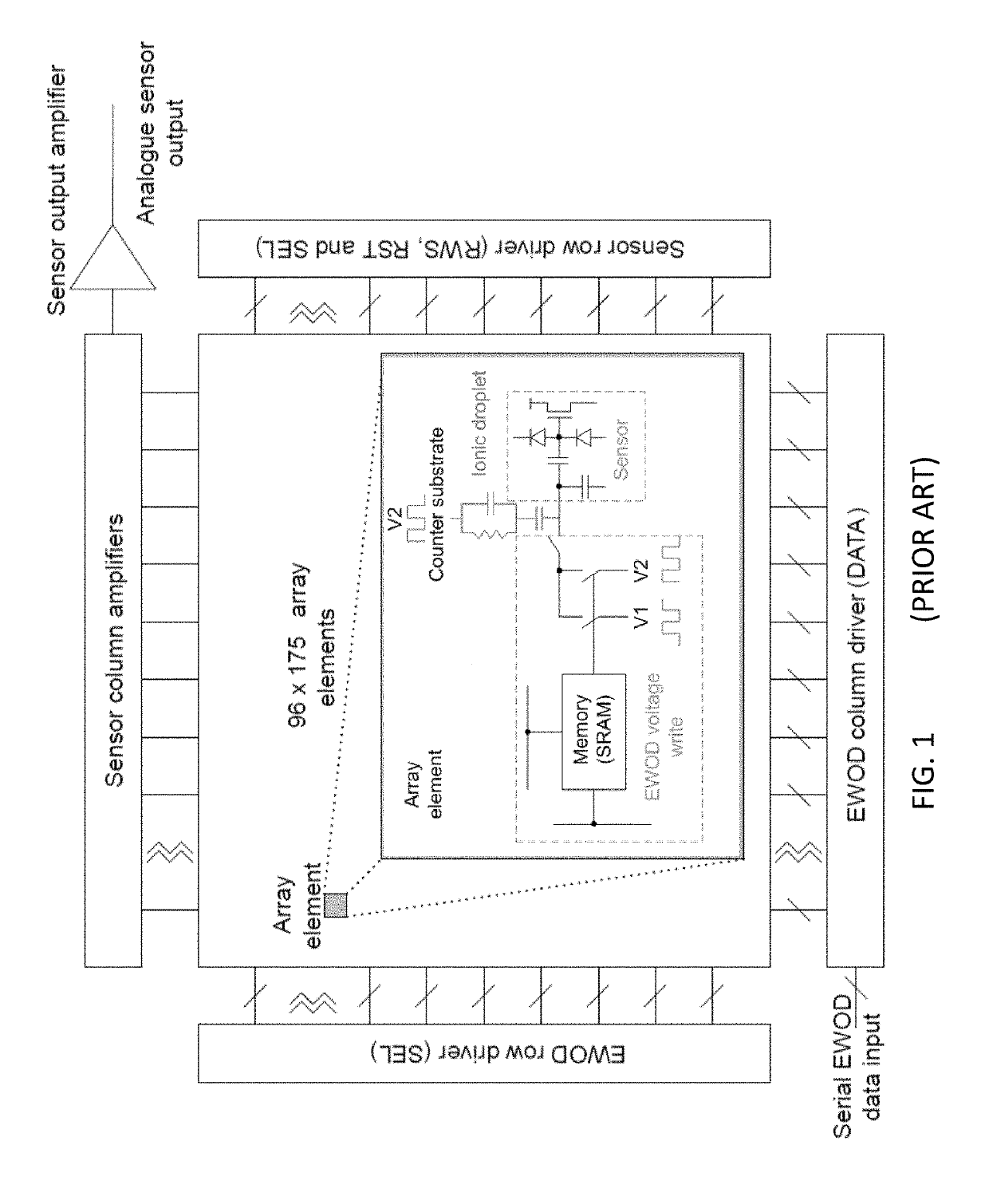
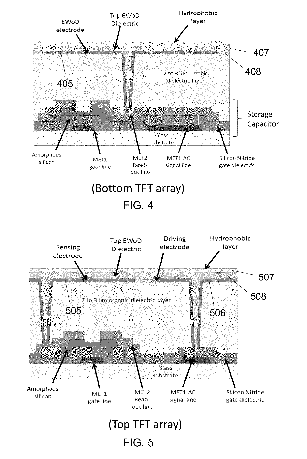
[0021]As indicated above, the present invention provides an active matrix electrowetting on dielectric (AM-EWoD) device including dual substrates with thin-film transistors (TFT) and capacitive sensing. As depicted herein the “bottom” substrate includes a plurality of electrodes to propel various droplets through a microfluidic region. The “top” substrate includes a plurality of electrodes to provide a signal and to detect the presence and / or size and / or composition of a droplet with capacitive sensing. The use of “top” and “bottom” is merely a convention as the locations of the two substrates can be switched, and the devices can be oriented in a variety of ways, for example, the top and bottom plates can be roughly parallel while the overall device is oriented so that the substrates are normal to a work surface (as opposed to parallel to the work surface as shown in the figures). The top or the bottom substrate may include additional functionality, such as resistive heating and / or ...


PUM


Abstract

An active matrix electrowetting on dielectric (AM-EWoD) device including dual substrates with thin-film transistors (TFT) and capacitive sensing. As depicted herein the bottom substrate includes a first plurality of electrodes to propel various droplets through a microfluidic region, while the top substrate includes a second plurality of electrodes that are configured to interrogate the droplets with capacitive sensing. In some embodiments, the top substrate has zones of high-resolution sensing and zones of low-resolution sensing.

Description

RELATED APPLICATIONS[0001]This application claims priority to U.S. Provisional Patent Application No. 62 / 573,846, filed Oct. 18, 2017. All patents and patent applications referenced in this specification are incorporated by reference in their entireties.BACKGROUND[0002]Digital microfluidic devices use independent electrodes to propel, split, and join droplets in a confined environment, thereby providing a “lab-on-a-chip.” Digital microfluidic devices are alternatively referred to as electrowetting on dielectric, or “EWoD,” to further differentiate the method from competing microfluidic systems that rely on electrophoretic flow and / or micropumps. A 2012 review of the electrowetting technology was provided by Wheeler in “Digital Microfluidics,”Annu. Rev. Anal. Chem. 2012, 5:413-40, which is incorporated herein by reference in its entirety. The technique allows sample preparation, assays, and synthetic chemistry to be performed with tiny quantities of both samples and reagents. In rece...

Claims


Application Information

Patent Timeline
Patent Type & Authority Applications(United States)
IPC IPC(8): B01L3/00H01L27/12G02B26/00G09G3/34G01R27/26
CPCB01L3/502792B01L3/50273H01L27/1251H01L27/1248G02B26/005G09G3/348G01R27/2605B01L2400/0427B01L2300/161B01L3/5027B01L2200/0673H01L27/1255G02B21/0076B01L3/502707B01L3/502715B01L2300/0636B01L2300/0645B01L2300/165B01L3/502784
Inventor FRENCH, IAN
Owner NUCLERA LTD
Why Eureka
Try Eureka