Variable electrode size area arrays on thin-film transistor based digital microfluidic devices for fine droplet manipulation

a technology of thin-film transistors and microfluidic devices, applied in fluid controllers, laboratory glasswares, laboratory apparatus, etc., can solve the problems of requiring faster (and more expensive) drivers, unable to perform massive parallel assays, reactions, etc., and limited number of electrodes, etc., to achieve the effect of simplifying the fabrication of the device and simplifying the data handling associated

Pending Publication Date: 2021-06-10
NUCLERA LTD
View PDF0 Cites 1 Cited by
  • Summary
  • Abstract
  • Description
  • Claims
  • Application Information

AI Technical Summary

Benefits of technology

[0006]The present application addresses the shortcomings of the prior art by providing an alternate architecture for an AM-EWoD with variable electrode size areas. In one instance, the invention provides a digital microfluidic device having two areas of different electrode densities, i.e., a high-density (a.k.a. “high-res”) area, and a low density (a.k.a. “low-res”). Such a design will allow a user to perform droplet manipulation where needed. Overall, such a configuration simplifies the fabrication of a device while also simplifying the data handling associated with the sensing functions.

Problems solved by technology

While segmented devices are easy to fabricate, the number of electrodes is limited by space and driving constraints.
Accordingly, it is not possible to perform massive parallel assays, reactions, etc. in direct drive devices.
Having high density electrodes at all locations requires faster (and more expensive) drivers and also increase the amount of data processing required.
Nonetheless, combining smaller electrodes to represent larger ones increases the complexity of the system due to the increased number of drive lines and data requirements.
It discloses electrode sub-arrays of 8 different sizes, however, the architecture of the '823 publication is not suitable to create subarrays of different sized electrodes on the same TFT platform due to drive line and geometry requirements.

Method used


Image

  • Variable electrode size area arrays on thin-film transistor based digital microfluidic devices for fine droplet manipulation
  • Variable electrode size area arrays on thin-film transistor based digital microfluidic devices for fine droplet manipulation
  • Variable electrode size area arrays on thin-film transistor based digital microfluidic devices for fine droplet manipulation

Examples


example 1

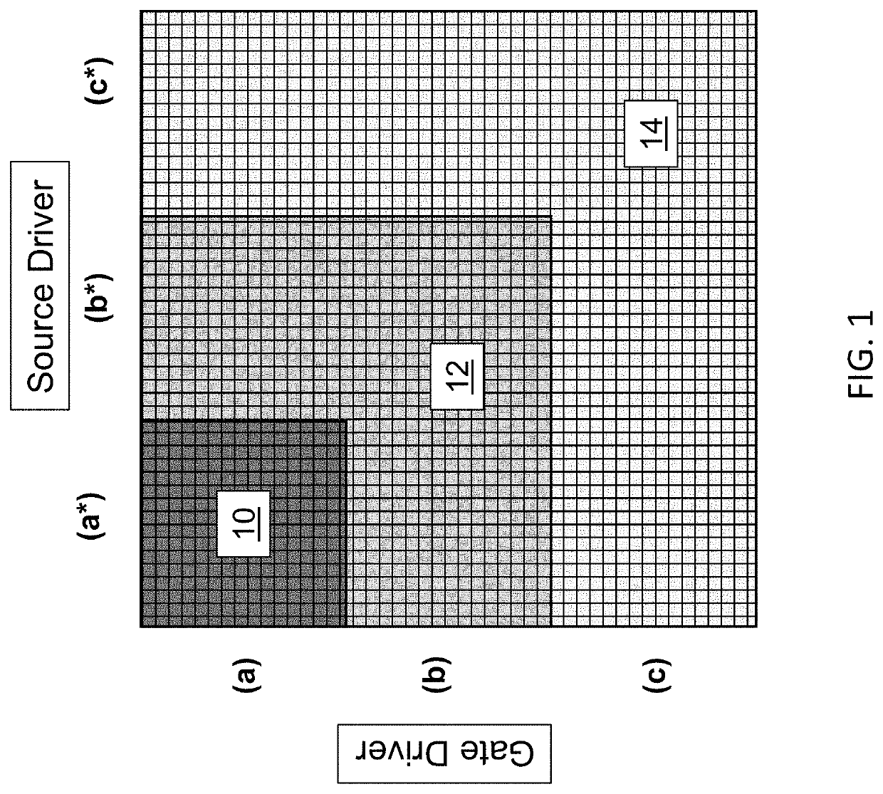
[0035]The diagram of FIG. 1 illustrates the structure of an exemplary variable size electrode array. The array is partitioned into three areas 10, 12, and 14, where the subarray of each area is defined by its respective drive line density a, b, or c. While the areas of FIG. 1 have the same row and column line density, this is not a requirement. For instance, area 10 may be characterized by row line density a, but also by a column line density a*, which may be greater or lesser than a, depending on the requirements of the application at hand. In one exemplary implementation, lower density areas branch away from a high-density area. In addition, if desired, the gate and source lines may be terminated to adjust for a desired density as one ventures deeper into the array to avoid extra capacitance in the lower density areas arising from the high-density lines. The advantage to this design feature is the ability to carry out high-resolution operations on the array at reduced gate and / or ...

example 2

[0037]Illustrated in FIG. 6 is the structure of another exemplary variable size array. Area 50 is of line density (row and column) a, and area 32 is of line density b. Line density a is greater than b. As such, if D1 is defined as the electrode density of area 50, as expressed for instance in terms of number of electrodes per 100 mm2, and D2 is defined as the electrode density of area 52, then the ratio D1:D2 exceeds the value of 1. In representative embodiments, the ratio D1:D2 is equal to about 2′, n being a natural number, so as to maintain a square electrode format. For example, the ratio D1:D2 may be equal to about 2, 4, 8, or 16 to suit the application at hand. The size of individual electrodes in AM-EWoD devices usually falls in a range from about 50 μm to about 600 μm. Hence, if the electrodes of area 52 are 600 μm in size, those of area 50 may be 300, 150, or 75 μm depending on whether the desired ratio D1:D2 is 2, 4, or 8.

[0038]Embodiments where the D1:D2 ratio is equal to...

example 3

[0040]The schematic drawing of FIG. 7 illustrates an example AM-EWoD device 60. Reservoirs R1 contain a first type of fluid, reservoirs R2 a second type of fluid, and reservoir R3 a third type of fluid. The TFT array of the device includes high electrode density areas 62 in the proximity of the reservoir inlets, so that sample droplets can be taken from a reservoir and deposited on the surface of a high electrode density area. The high electrode density of the subarrays of areas 62 enables carrying out assay steps such as diluting, mixing, and sizing (splitting) of sample droplets with high accuracy. In one example embodiment, a sample droplet to be assayed for the presence and optionally the concentration of an analyte to is diluted by combination with one or more droplets of a solvent, and the dilution step may be repeated until a desired analyte concentration range is attained. Then, a droplet of the diluted sample is mixed with droplet(s) of one or more reactants that form a det...


PUM

PropertyMeasurementUnit
sizeaaaaaaaaaa
sizeaaaaaaaaaa
areaaaaaaaaaaa

Abstract

A digital microfluidic device including a substrate and a controller. The substrate includes: a first high-resolution area and a second low-resolution area, and a hydrophobic layer. The first area includes a first plurality of electrodes having a first density D1, and a first set of thin-film-transistors coupled to the first plurality of electrodes. The second area includes a second plurality of electrodes having a second density D2, where D2<D1, and a second set of thin-film-transistors coupled to the second plurality of electrodes. The hydrophobic layer covers both the first and second pluralities of electrodes and the first and second sets of thin-film-transistors. The controller is operatively coupled to the first set and second set of thin-film-transistors and configured to provide a propulsion voltage to at least a portion of the first plurality of electrodes and at least a portion of the second plurality of electrodes.

Description

RELATED APPLICATIONS[0001]This application claims priority to U.S. Provisional Patent Application No. 62 / 943,295, filed Dec. 4, 2019. All patents and publications disclosed herein are incorporated by reference in their entireties.BACKGROUND[0002]Digital microfluidic devices use independent electrodes to propel, split, and join droplets in a confined environment, thereby providing a “lab-on-a-chip.” Digital microfluidic devices are alternatively referred to as electrowetting on dielectric, or “EWoD,” to further differentiate the method from competing microfluidic systems that rely on electrophoretic flow and / or micropumps. A 2012 review of the electrowetting technology was provided by Wheeler in “Digital Microfluidics,”Annu. Rev. Anal. Chem. 2012, 5:413-40, which is incorporated herein by reference in its entirety. The technique allows sample preparation, assays, and synthetic chemistry to be performed with tiny quantities of both samples and reagents. In recent years, controlled dro...

Claims


Application Information

Patent Timeline
Patent Type & Authority Applications(United States)
IPC IPC(8): B01L3/00
CPCB01L3/502784B01L2400/0415B01L2300/161B01L3/502792B01L2200/023B01L2200/12
Inventor ZHITOMIRSKY, DAVIDPAOLINI, JR., RICHARD J.FRENCH, IANO'MALLEY, TIMOTHY J.
Owner NUCLERA LTD
Why Eureka
Try Eureka