

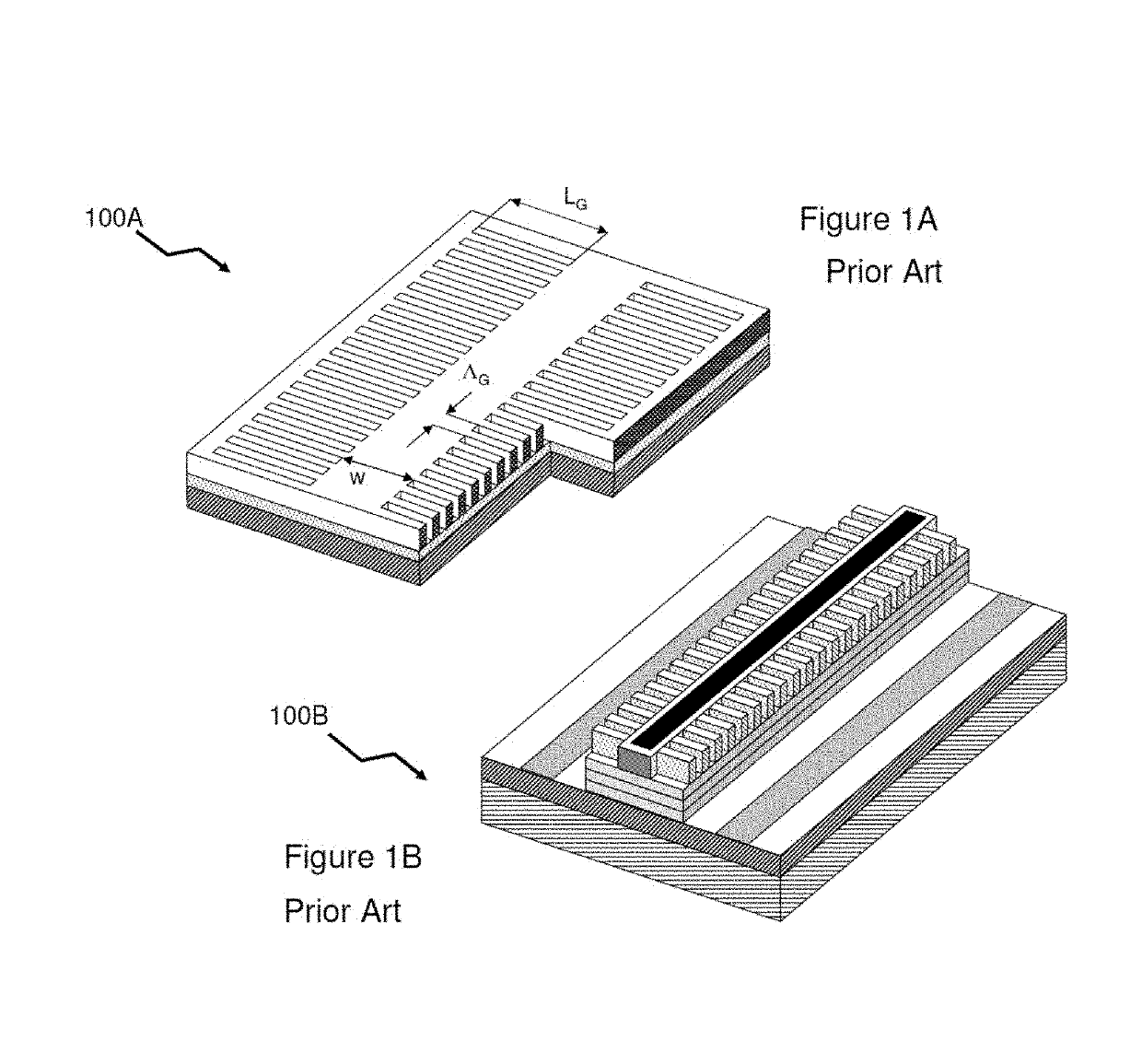
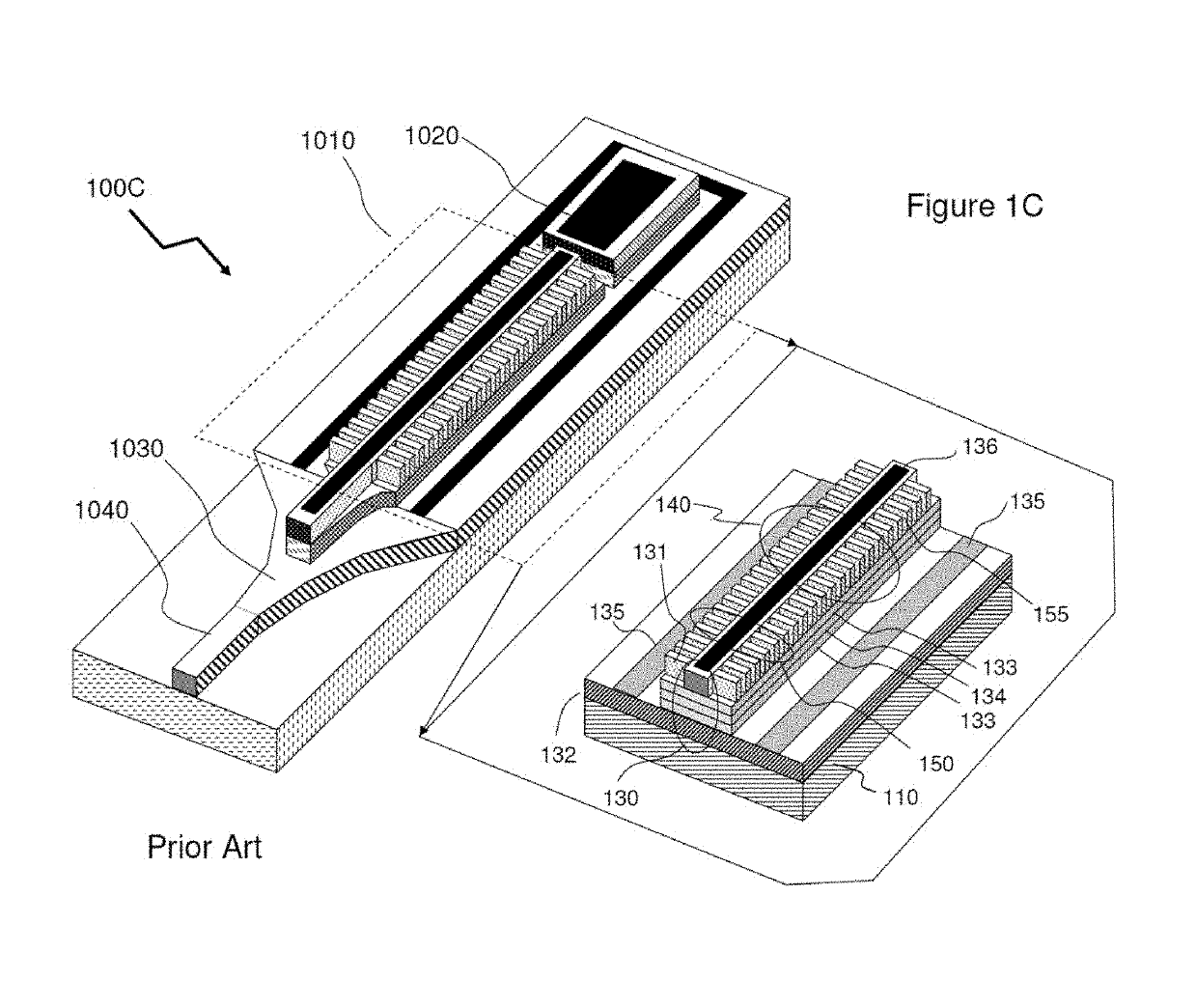
Vertically-coupled surface-etched grating dfb laser
a grating and laser technology, applied in the field of semiconductor lasers, to achieve the effect of enhancing laser performance, optimizing injection current overlap, and increasing injection efficiency
- Summary
- Abstract
- Description
- Claims
- Application Information
AI Technical Summary
Benefits of technology
Problems solved by technology
Method used
Image

Examples
first embodiment
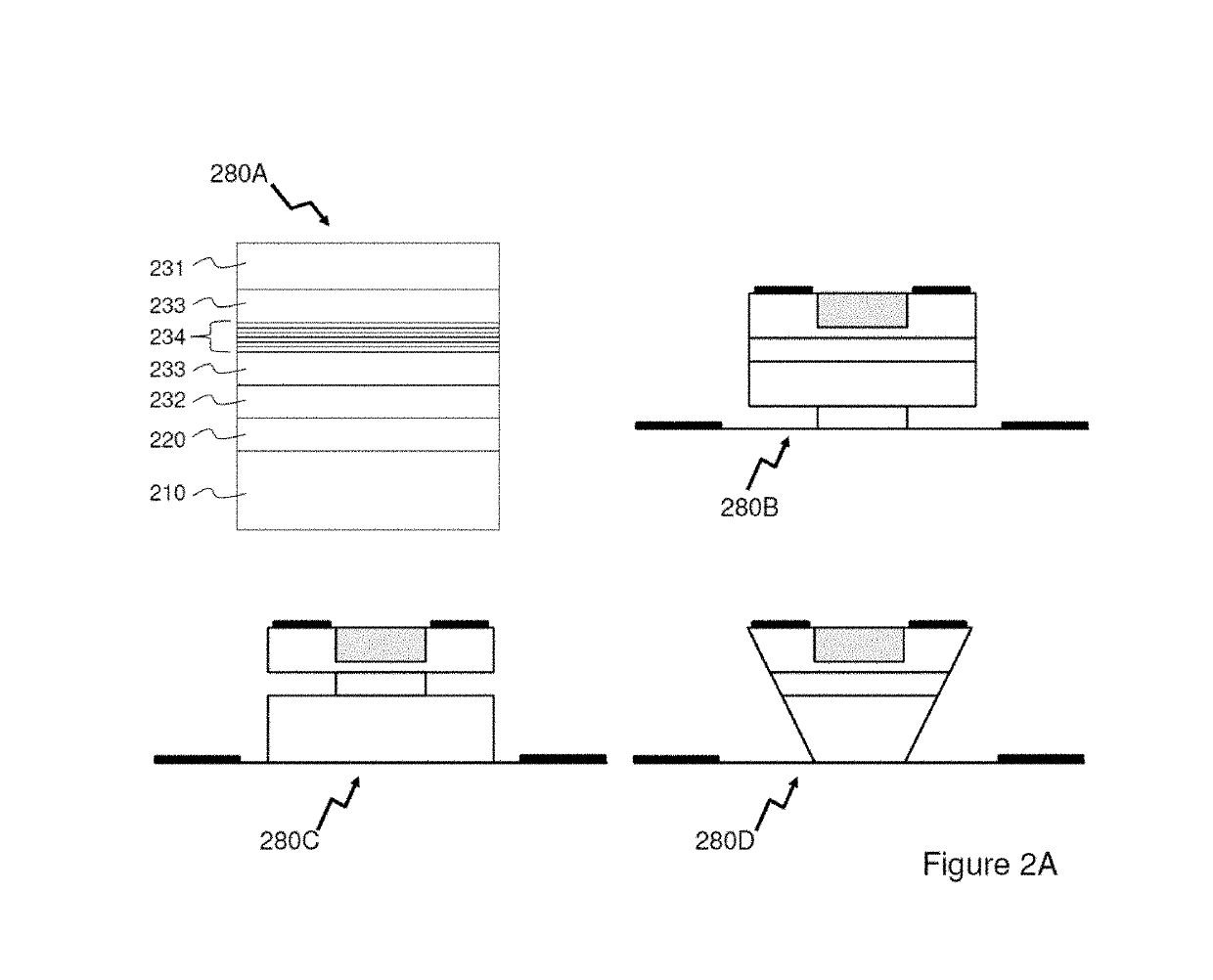
[0042]In the the invention illustrated by the first laser mesa's cross-section 280A shown schematically in FIG. 2A, the lateral confinement for both the optical field and injection current is achieved by a lateral undercut of the semiconductor material at the bottom of the mesa. In practice, such a lateral undercut in InP-based material system is implementable by inserting a GaxIn1-xAsyP1-y or AlxGayIn1-x-yAs layer in between two InP layers and using highly selective chemical (wet) etcher that etches GaxIn1-xAsyP1-y or AlxGayIn1-x-yAs at a rate much higher than it etches InP. This process, even though as that used in different configurations and for different purposes, is well documented in a prior art, e.g. by Z.-Z. Liau, et al in the U.S. Pat. No. 4,468,850, where the GaInAsP active layer sandwiched between P- and N-emitter InP layers and positioned in the vertical stack at the bottom of the P-up / N-down edge-emitting laser mesa grown on N+-InP substrate was undercut to form a buri...
second embodiment
[0043]In the invention illustrated by the second laser mesa's cross-section 280C shown schematically in FIG. 2A, the lateral confinement for both the optical field and injection current is achieved by a lateral undercut of the semiconductor material of some of SCH layers, e.g. active MQW layers, in the middle of the mesa. Since these layers, by default, have to have narrower bandgap and hence higher refractive index that N- and P-InP emitter layers on both sides of the SCH, they must be made from the materials other than InP, most commonly GaxIn1-xAsyP1-y and AlxGayIn1-x-yAs materials, which, again, can be used for a lateral undercut by means of selective chemical (wet) etching. Examples of such a process can be found in a in prior art, e.g. in the paper by D. Pasquariello et al entitled “Selective Undercut Etching of InGaAs and InGaAsP Quantum Wells for Improved Performance of Long-Wavelength Optoelectronic Devices”, J. Lightwave Technol., Vol. 24, No 3, P. 1470 (2006) and paper by...
third embodiment
[0044]In the invention illustrated by the third laser mesa's cross-section 280D shown schematically in FIG. 2C, the lateral confinement for both the optical field and injection current is achieved by means of a selective anisotropic wet etching, first, the upper N-InP emitter layer down to the SCH layers and, second, the SCH layers, down to the lower P-InP emitter layer. In such a process, e.g. as reported by M. Aoki et al in the paper entitled “InP-Based Reversed-Mesa Ridge-Waveguide Structure for High-Performance Long-Wavelength Laser Diodes” (IEEE J. Selective Topics in Quantum Electron, Vol. 3, No. 2, pp. 672 (1997)).
[0045]The above-described embodiments of the present invention are intended to be examples only, as it concerns to the arrangements for providing the lateral confinement to the optical field below the SEG region—a must in the VCSEG-DFB construction that, opposite to its LCSEG-DFB counterpart, lacks the lateral optical confinement in the SEG area and also to the inje...
PUM
 Abstract
Description
Claims
Application Information