Semiconductor device and method of manufacturing same

a semiconductor and semiconductor technology, applied in the direction of semiconductor devices, basic electric elements, electrical apparatus, etc., can solve the problems of insufficient arrangement position of barrier layers, and achieve the effects of preventing diffusion, stable electrical characteristics, and high reliability

Active Publication Date: 2019-04-18
FUJI ELECTRIC CO LTD
View PDF0 Cites 2 Cited by
  • Summary
  • Abstract
  • Description
  • Claims
  • Application Information

AI Technical Summary

Benefits of technology

[0007]The present invention, in view of the aforementioned problem, aims at providing a semiconductor device with stable electrical characteristics and high reliability by preventin

Problems solved by technology

In Patent Documents 1 and 2, the arrangement position of the barrier layer is

Method used


Image

  • Semiconductor device and method of manufacturing same
  • Semiconductor device and method of manufacturing same
  • Semiconductor device and method of manufacturing same

Examples


Embodiment Construction

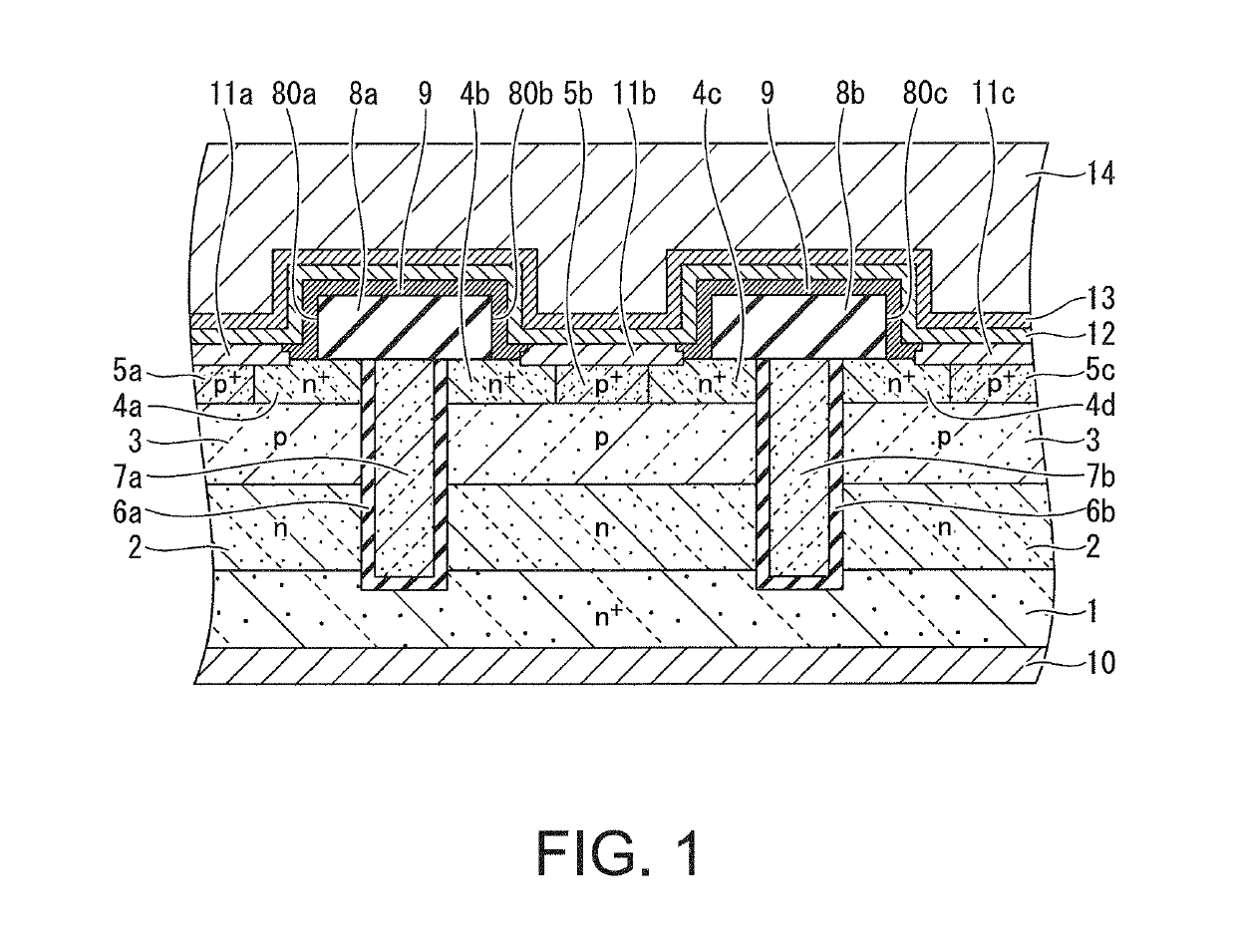
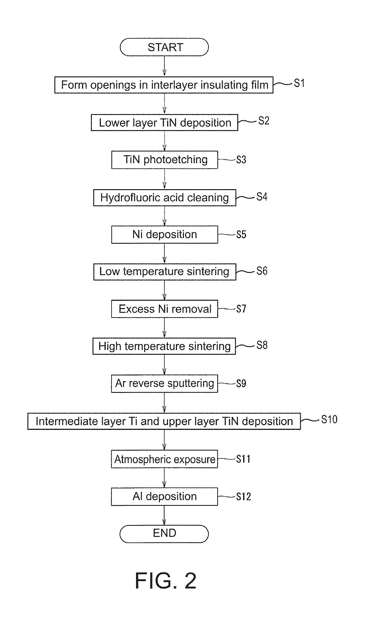
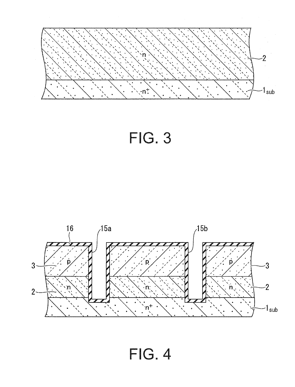
[0028]An embodiment of the present invention will be explained below with reference to the drawings. In the drawings, portions that are the same or similar will be assigned the same or similar reference characters and redundant explanations will be omitted. However, the drawings are schematic, and the relationship between thickness and planar dimensions, the ratio of the thickness of each layer, etc. may differ from practice. Furthermore, there can be parts for which the relationship between dimensions, ratios, etc. differ even among the drawings. The embodiment shown below illustratively indicates a device and method for carrying out the technical idea of the present invention, and the technical idea of the present invention is not limited to the material, shape, structure, arrangement, etc. of the constituent components described below.

[0029]In addition, the definition of directions such as up-down in the description below are merely definitions for convenience of explanation and ...


PUM


Abstract

A semiconductor device includes a first barrier film covering the main surface of the active region and the insulating film layer, the first barrier film having an ohmic contact hole that exposes a contact portion of the ohmic contact formation region within the window of the insulating film layer; a base contact layer filled into the ohmic contact hole and making ohmic contact with the contact portion of the ohmic contact formation region; a second barrier film made of titanium, covering the base contact layer and the first barrier film; and a third barrier film made of titanium oxide and titanium nitride, covering a surface of the second barrier film.

Description

BACKGROUND OF THE INVENTIONTechnical Field[0001]The present invention relates to an electrode structure of a semiconductor device and a method of manufacturing the same.Background Art[0002]The main electrode region, such as the source region or drain region, provided in the active region of a semiconductor device is electrically connected to an ohmic electrode. In this case, an insulating film layer such as an interlayer insulating film is selectively disposed between the ohmic electrode and the active region, and ohmic contact is made at a window part provided in the insulating film layer. If the metal or hydrogen contained in the ohmic electrode in this type of structure diffuses to the insulating film layer and the active region, then the electric boundary conditions of the semiconductor device will fluctuate, and electrical characteristics such as the threshold voltage will fluctuate.[0003]Patent Document 1 proposes a method for reducing threshold fluctuations by using, for an i...

Claims


Application Information

Patent Timeline
IPC IPC(8): H01L29/45H01L29/51H01L29/423H01L21/8234
CPCH01L29/45H01L29/51H01L29/4236H01L21/823443H01L29/7397H01L29/7813H01L29/7455H01L29/7396H01L29/66348H01L29/401H01L29/417H01L29/456H01L29/66734H01L29/41725
Inventor UTSUMI, MAKOTOSAKAI, YOSHIYUKI
Owner FUJI ELECTRIC CO LTD
Why Eureka
Try Eureka