Preparation method for printing OLED display
a technology of oled display and printing method, which is applied in the field of oled display, can solve the problems of high cost, failure to define rgb sub-pixels, complex process, etc., and achieve the effect of improving the production yield of printing
- Summary
- Abstract
- Description
- Claims
- Application Information
AI Technical Summary
Benefits of technology
Problems solved by technology
Method used
Image


Examples
Embodiment Construction
[0023]To facilitate the understanding of those skilled in the art, the invention will be further illustrated in details below in conjunction with the accompanying drawings and particular embodiments.
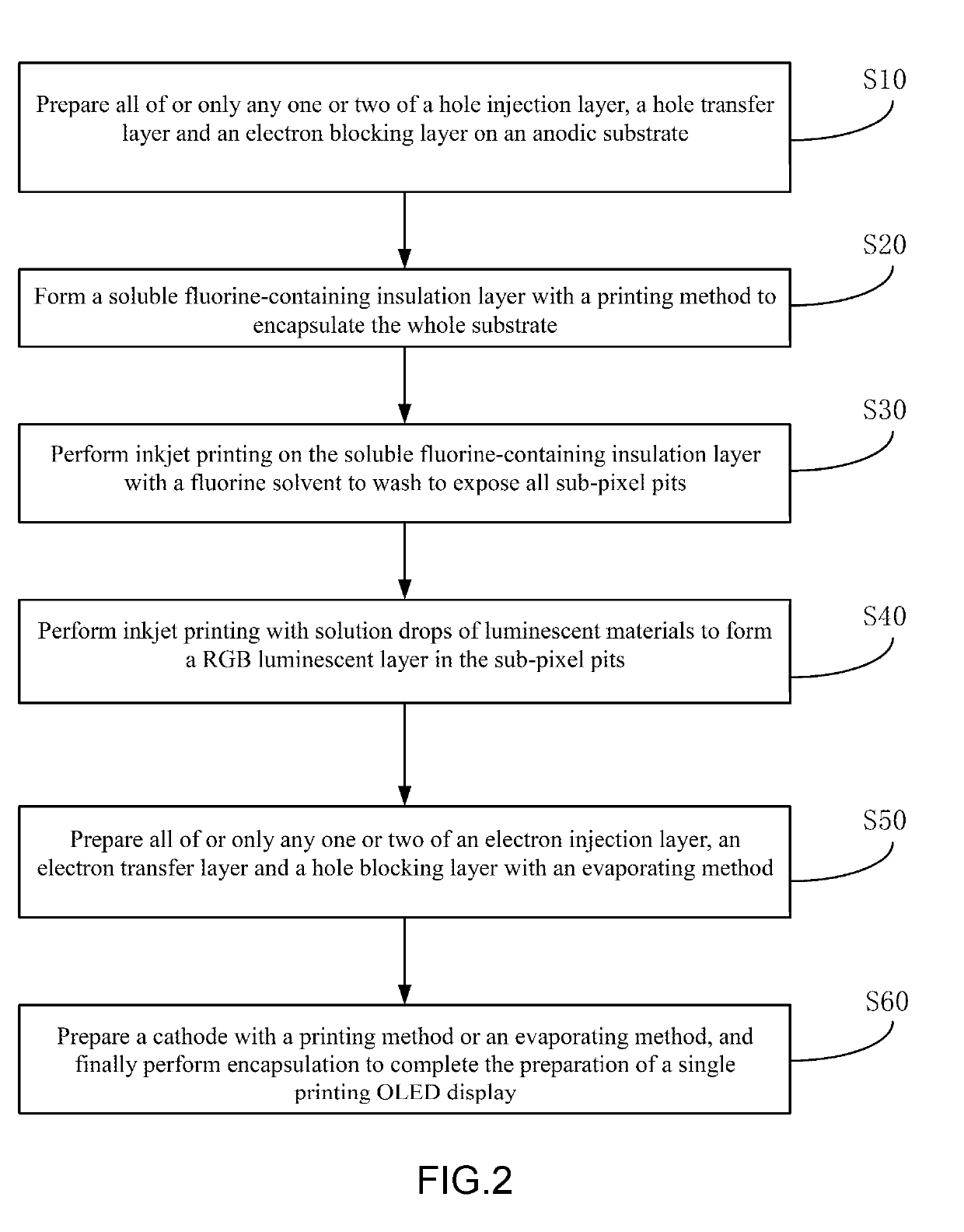
[0024]As shown in FIG. 2, a preparation method for a printing OLED display comprises the following steps.
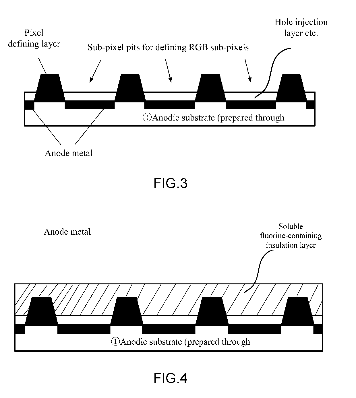
[0025]S10. Prepare all of or only any one or two of a hole injection layer, a hole transfer layer and an electron blocking layer on an anodic substrate, where the selection on the specific layer(s) to be prepared is made according to actual needs;
[0026]moreover, the hole injection layer, the hole transfer layer or the electron blocking layer can be prepared with a printing method or an evaporating method, and the hole injection layer, the hole transfer layer or the electron blocking layer has the thickness preferably of 5-100 nm.
[0027]For instance, the printing method (inkjet printing, screen printing, spin coating, spray coating, blade coating, imprinting etc.) can be applied to the ...
PUM
 Abstract
Description
Claims
Application Information
 - R&D
- Intellectual Property
- Life Sciences
- Materials
- Tech Scout
- Unparalleled Data Quality
- Higher Quality Content
- 60% Fewer Hallucinations
Browse by: Latest US Patents, China's latest patents, Technical Efficacy Thesaurus, Application Domain, Technology Topic, Popular Technical Reports.
© 2025 PatSnap. All rights reserved.Legal|Privacy policy|Modern Slavery Act Transparency Statement|Sitemap|About US| Contact US: help@patsnap.com