Transistor laser electrical and optical bistable switching

a technology of optical bistable switching and transistor laser, which is applied in the direction of lasers, optics, semiconductor lasers, etc., can solve the problems of inability to apply optics to digital computers, limited bandwidth of digital electronic computers, and lack of suitable optical logic processors with scalable size and speed

Active Publication Date: 2019-04-25
THE BOARD OF TRUSTEES OF THE UNIV OF ILLINOIS
View PDF1 Cites 2 Cited by
  • Summary
  • Abstract
  • Description
  • Claims
  • Application Information

AI Technical Summary

Benefits of technology

[0009]Due to the “planar” geometry of the transistor structure, the active devices or passive components can be conveniently replicated into electrical logic building blocks (ICs) for computing and for all other traditional (electronics) information processing functions. The uniqueness of the transistor laser and its “third” port, an optical dimension, is convenient for ICs and computer. All the required components can be fabricated on a single epitaxial structure for transistor, laser, detector, and IC replication, thus facilitating the electronic-photonics integrated circuits (EOICs) on a very large scale. The transistor laser fundamentally enables the development of high-speed digital computation in the optical domain. It possesses the unique 3-port electrical and optical, characteristics for directly current or voltage modulation and allows the design of ultra-high-speed integrated optical switches (see e.g. M. Feng, Han Wui Then, and Nick Holonyak, Jr., “Transistor Laser Optical NOR Gate for High Speed Optical Logic Processors,”GOMACTech-2017 (Session 8: Beyond CMOS Technologies (Paper No. 8.4))-Reno, Nev., Mar. 21-(2017) and see also M. Feng, J. Qiu, C. Y. Wang, and N. Holonyak, Jr., J. Appl. Phys. 120, 20451 (2016)).

Problems solved by technology

Today, digital electronic computers are bandwidth limited by the signal delay of RC time constants and carrier transit times of electronic logic.
However, the full application of optics has yet to be applied to digital computers for reasons including the lack of suitable optical logic processors with scalable size and speed.
However, the major issue with a laser-photothyristor pair is that the PNPN-thyristor stores charge and has a very slow switching speed, typically in the MHz range.
This fundamental limitation is owing to the saturated nature of the PNPN switching operation.
Once turned on, the PNPN device accumulates large quantities of charge in its base, and takes a long time to turn off.
This sets a fundamental limit to the speed of the laser-photothyristor to MHz switching.
Other approaches based on external optical components such as semiconductor optical amplifiers (SOA), electro-absorption modulators (EAM) and Mach-Zehnder modulators (MZM) are limited by low coupling efficiencies and low extinction ratios.
Such difficulties and large device dimensions (˜mm) are difficult for achieving high density integrated designs as required for logic applications.
However, previous studies have not included the effect of electro-optical cavity coupling and quality Q. In the transistor laser, the coherent photons generated at the base quantum-well interact with the collector field and “assist” optical cavity electron tunneling from the base valence band to the adjacent conduction band of the collector junction.

Method used


Image

  • Transistor laser electrical and optical bistable switching
  • Transistor laser electrical and optical bistable switching
  • Transistor laser electrical and optical bistable switching

Examples


Embodiment Construction

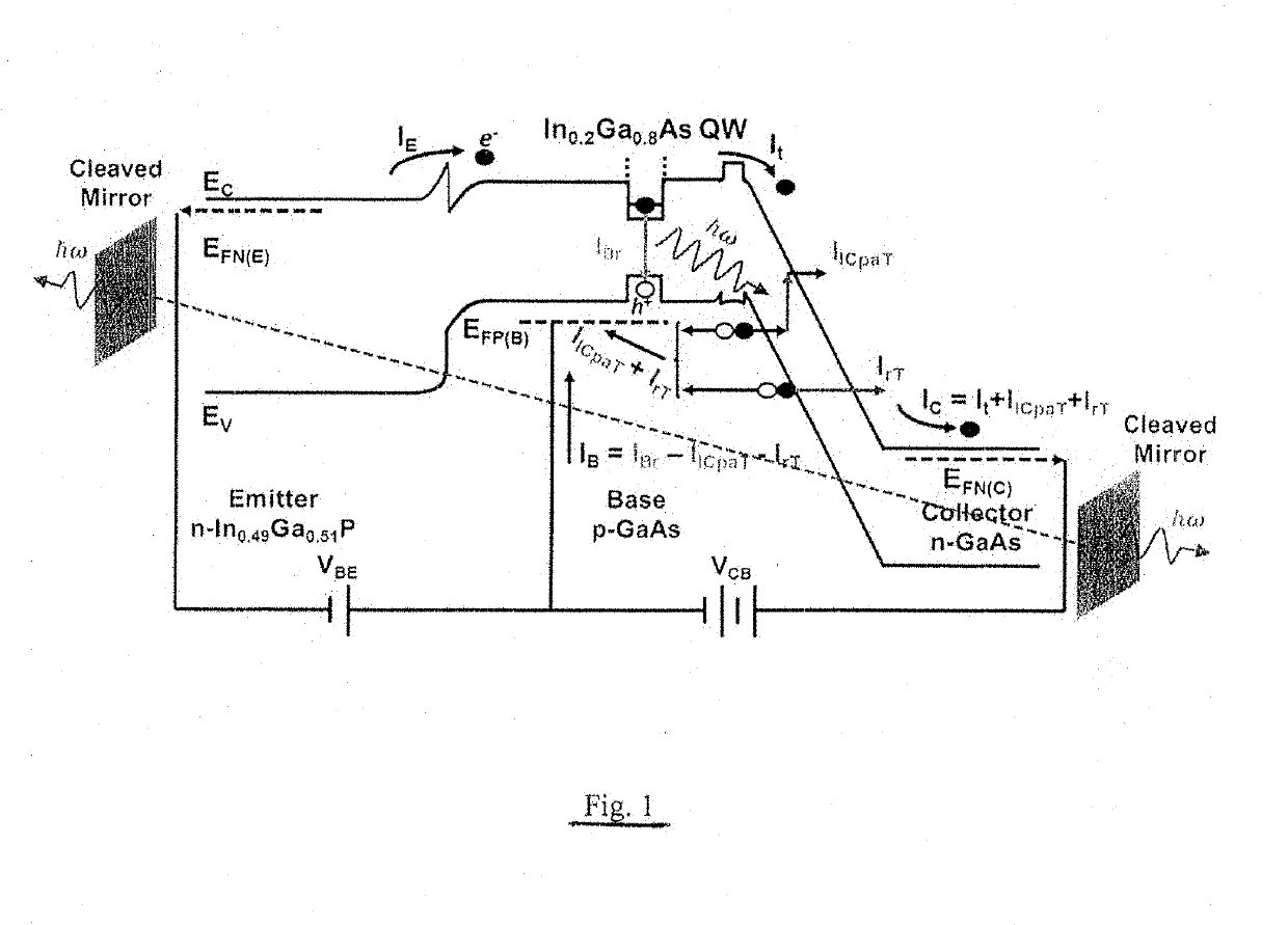
[0029]The schematic energy band diagram of a heterojunction transistor laser (n-p-n) with a quantum-well (QW) in the base, photon-assisted tunneling at the collector junction, and a reflecting optical cavity are shown in FIG. 1 operating with emitter current injection, base recombination and transport, and tunneling collector current. The base recombination hole current (IBr) is supplied by the external base current (IB), the intracavity photon-assisted tunneling hole current (IICPAT, h), and the band-to-band tunneling hole current (IrT). The collector electron current (IC) is contributed from the base electron current reaching the collector junction (It), the intracavity photon-assisted tunneling electron current (IICPAT, e), and the band-to-band tunneling electron current (IrT). The photon generation is due to e-h recombination at base quantum-well, and the photon absorption is due to intra-cavity photon-assisted e-h tunneling at the collector junction. The corresponding hole curr...


PUM


Abstract

A method for electrical and optical bistable switching, including the following steps: providing a semiconductor device that includes a semiconductor base region of a first conductivity type between semiconductor collector and emitter regions of a second conductivity type, providing a quantum size region in the base region, and providing base, collector and emitter terminals respectively coupled with the base, collector, and emitter regions; providing input electrical signals with respect to the base, collector, and emitter terminals to obtain an electrical output signal and light emission from the base region; providing an optical resonant cavity that encloses at least a portion of the base region and the light emission therefrom, an optical output signal being obtained from a portion of the light in the optical resonant cavity; and modifying the input electrical signals to switch back and forth between a first state wherein the photon density in the cavity is below a predetermined threshold and the optical output is incoherent, and a second state wherein the photon density in the cavity is above the predetermined threshold and the optical output is coherent, said switching from the first to the second state being implemented by modifying the input electrical signals to reduce optical absorption by collector intra-cavity photon-assisted tunneling, and the switching from the second to the first state being implemented by modifying the input electrical signals to increase photon absorption by collector intra-cavity photon-assisted tunneling.

Description

BACKGROUND OF THE INVENTION[0001]Included in the background hereof are the teachings of U.S. Pat. No. 9,478,942 of M. Feng, N. Holonyak, Jr., and M. K. Wu, assigned to the same assignee as the present Application, and incorporated herein by reference. Reference can also be made to documents cited therein, including: U.S. Pat. Nos. 7,091,082, 7,286,583, 7,354,780, 7,535,034, 7,693,195, 7,696,536, 7,711,015, 7,813,396, 7,888,199, 7,888,625, 7,953,133, 7,998,807, 8,005,124, 8,179,937, 8,179,939, 8,494,375, and 8,509,274; U.S. Patent Application Publication Numbers US2005 / 0040432, US2005 / 0054172, US2008 / 0240173, US2009 / 0134939, US2010 / 0034228, US2010 / 0202483, US2010 / 0202484, US2010 / 0272140, US2010 / 0289427, US2011 / 0150487, and US2012 / 0068151; and to PCT International Patent Publication Numbers WO / 2005 / 020287 and WO / 2006 / 093883 as well as to the publications referenced in U.S. Patent Application Publication Number US2012 / 0068151.[0002]Bistability occurs in electrical or optical systems in...

Claims


Application Information

Patent Timeline
Patent Type & Authority Applications(United States)
IPC IPC(8): H01S5/062H01S5/183H01S5/34H01S5/30H01S5/32H01S5/343H01L33/00
CPCH01S5/06203H01S5/183H01S5/3415H01S5/06226H01S5/3407H01S5/3054H01S5/3211H01S5/34313H01L33/0025G02F3/026
Inventor FENG, MILTONHOLONYAK, JR., NICKWU, MONG-KAITAN, FEI
Owner THE BOARD OF TRUSTEES OF THE UNIV OF ILLINOIS
Why Eureka
Try Eureka