Unlock instant, AI-driven research and patent intelligence for your innovation.

C-axis aligned crystalline igzo thin film and manufacture method thereof

a technology of crystalline igzo and manufacturing method, which is applied in the field of display technology, can solve the problems of poor stability of tft, complicated manufacturing process of low temperature poly silicon thin film transistor production line, and large yield problems, and achieve the effect of raising the stability of tft and large-scale application

Inactive Publication Date: 2019-05-23
WUHAN CHINA STAR OPTOELECTRONICS TECH CO LTD
View PDF14 Cites 1 Cited by
  • Summary
  • Abstract
  • Description
  • Claims
  • Application Information

AI Technical Summary

Benefits of technology

The present invention provides a manufacturing method for a C-axis Aligned Crystalline IGZO thin film with improved crystal quality and reduced oxygen defects, which improves the stability of TFTs. The larger area of the crystalline region in the manufactured film advantageously promotes its large scale application. The method utilizes atomic layer deposition to accurately control the structure of the thin film at the atomic level and includes optimized process conditions to improve production yield and decrease production cost. The C-axis Aligned Crystalline IGZO thin film has fine crystal quality, reduced oxygen defects, and larger crystalline region, which makes it advantageous for large scale applications.

Problems solved by technology

However, the manufacture process of the Low Temperature Poly Silicon Thin Film Transistor (LTPS TFT) production line is extremely complicated, and the yield is a major problem, too.
The biggest issue existing in the IGZO large scale use is that the rapid change of the vacancy oxygen (or oxygen defect) in IGZO will lead to the worse stability of TFT.
This is an issue caused by the defect of the IGZO material itself.
Because the area of the crystalline region is smaller, thus it is disadvantageous to the large scale application of the C-axis Aligned Crystalline IGZO.

Method used


Image

  • C-axis aligned crystalline igzo thin film and manufacture method thereof
  • C-axis aligned crystalline igzo thin film and manufacture method thereof
  • C-axis aligned crystalline igzo thin film and manufacture method thereof

Examples


Embodiment Construction

[0047]For better explaining the technical solution and the effect of the present invention, the present invention will be further described in detail with the accompanying drawings and the specific embodiments.

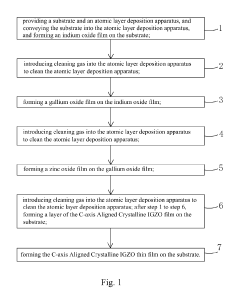
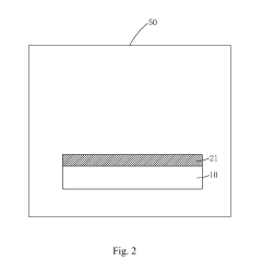
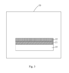
[0048]Atomic Layer Deposition (ALD) is a method of pulse alternately introducing the gas precursor into the reactor to form a deposition film on a substrate by chemical adsorption and reaction. When the precursors reach the surface of the substrate, they will have chemical adsorption on the surface and have the surface reaction. Between the precursor pulses, it is required to clean the atomic layer deposition reactor with the inactive gas. Obviously, whether the precursor material of the deposition reaction can be chemical adsorbed by the surface of the deposition material is the key to realize the atomic layer deposition. It can be seen from the adsorption characteristics of the gas phase material on the surface of the substrate, any gas phase material can conduct the physica...


PUM

PropertyMeasurementUnit
temperatureaaaaaaaaaa
pressureaaaaaaaaaa
temperatureaaaaaaaaaa

Abstract

The present invention provides a C-axis Aligned Crystalline IGZO thin film and a manufacture method thereof. In the manufacture method of the C-axis Aligned Crystalline IGZO thin film of the present invention, by utilizing the method of atomic layer deposition to manufacture the C-axis Aligned Crystalline IGZO thin film, the structure of the C-axis Aligned Crystalline IGZO can be accurately controlled in the atomic level, and the crystalline quality of the C-axis Aligned Crystalline IGZO is fine, and the oxygen defect is less, which can raise the stability of TFT; moreover, the area of the crystalline region in the C-axis Aligned Crystalline IGZO thin film is larger, which reaches up for micron level to millimeter level, and thus can promote the large scale application of the C-axis Aligned Crystalline IGZO; meanwhile, the present invention utilizes the optimized process condition to manufacture the C-axis Aligned Crystalline IGZO thin film.

Description

FIELD OF THE INVENTION[0001]The present invention relates to a display technology field, and more particularly to a C-axis Aligned Crystalline IGZO thin film and a manufacture method thereof.BACKGROUND OF THE INVENTION[0002]The Thin Film Transistor (TFT) is a main drive component in a Liquid Crystal Display (LCD) and an Active Matrix Organic Light-Emitting Diode (AMOLED) at present, and directly relates to the development direction of the high performance flat panel display device.[0003]With the rising of the terminal applications of smart phone and the tablet display, the high precision panel requirements over 250 PPI (Pixels Per Inch) gradually become tie-in trend, and more panel factories are urged to expand the production of the high precision Low Temperature Poly Silicon (LTPS) Thin Film Transistor. However, the manufacture process of the Low Temperature Poly Silicon Thin Film Transistor (LTPS TFT) production line is extremely complicated, and the yield is a major problem, too....

Claims


Application Information

Patent Timeline
Patent Type & Authority Applications(United States)
IPC IPC(8): C23C16/40C23C16/455H01L27/12H01L21/02
CPCC23C16/407C23C16/45529C23C16/45544H01L27/1225H01L21/02609H01L21/02565H01L21/0262H01L27/1262C23C16/40C23C16/45531H01L21/02554H01L21/02661C23C16/45534C23C16/4408H01L29/7869
Inventor WANG, XUANYUN
Owner WUHAN CHINA STAR OPTOELECTRONICS TECH CO LTD