A Comprehensive Framework for Protecting Intellectual Property in the Semiconductor Industry

a comprehensive framework and semiconductor technology, applied in the direction of instruments, digital transmission, securing communication, etc., can solve the problems of increasing exponentially, affecting the design quality of semiconductor products, so as to prevent (or inhibit) ic overproduction, the effect of preventing (or inhibiting) ic overproduction

a comprehensive framework and semiconductor technology, applied in the direction of instruments, digital transmission, securing communication, etc., can solve the problems of increasing exponentially, affecting the design quality of semiconductor products, so as to prevent (or inhibit) ic overproduction, the effect of preventing (or inhibiting) ic overproduction

US20190165935A1Active Publication Date: 2019-05-30UNIV OF FLORIDA RES FOUNDATION INC +1

Image

  • A Comprehensive Framework for Protecting Intellectual Property in the Semiconductor Industry
  • A Comprehensive Framework for Protecting Intellectual Property in the Semiconductor Industry
  • A Comprehensive Framework for Protecting Intellectual Property in the Semiconductor Industry

Examples


embodiment 1

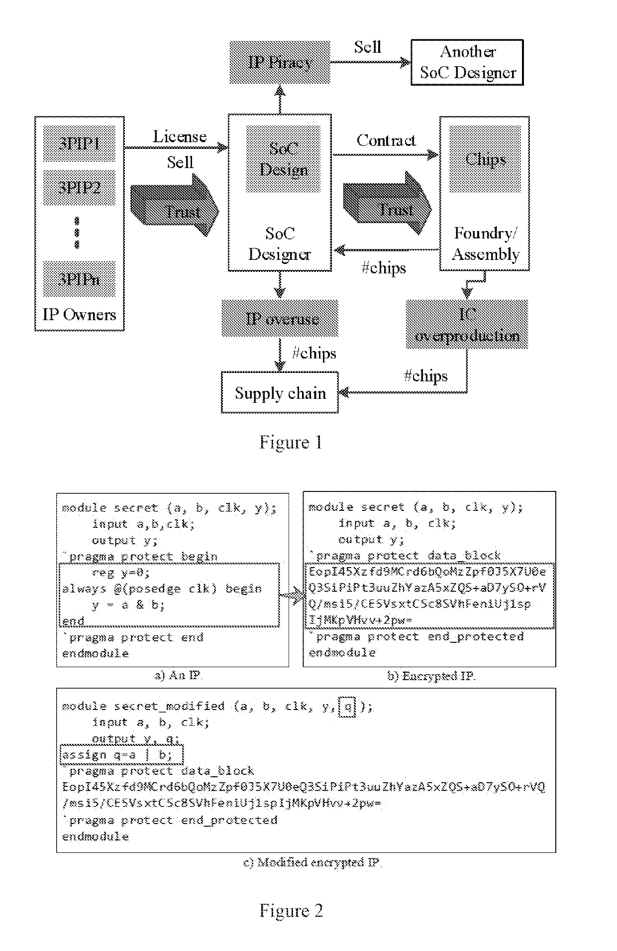
[0096]A method for preventing (or inhibiting) modification of IPs, the method comprising:

[0097]providing an IP (i.e., an item of intellectual property);

[0098]encrypting the IP with a random symmetric session key;

[0099]encrypting the random symmetric session key with a public key and attaching the encrypted random symmetric session key to the IP; and

[0100]adding an IP digest resulting from a cryptographic hash function in a IP header of the IP.

embodiment 100

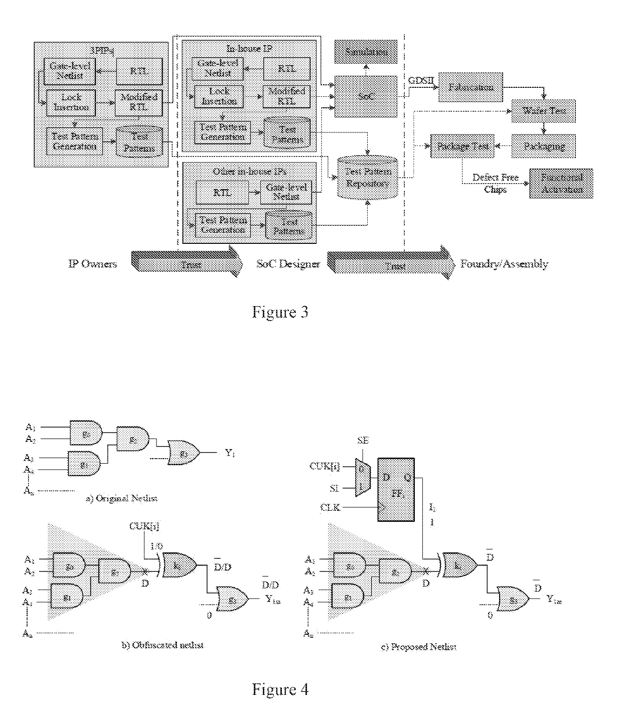
[0101]A method for preventing (or inhibiting) unauthorized overproduction of integrated circuits comprising a means for activating the integrated circuits after the integrating circuits have been tested.

embodiment 101

[0102]The method of embodiment 100, wherein the means for activating the integrated circuits after the integrated circuits have been tested includes: locking a design by using a set of key gates and that can only be unlocked upon receiving a valid chip unlock key (CUK).


PUM


Abstract

Methods and integrated circuit architectures for assuring the protection of intellectual property between third party IP providers, system designers (e.g., SoC designers), fabrication entities, and assembly entities are provided. Novel design flows for the prevention of IP overuse, IP piracy, and IC overproduction are also provided. A comprehensive framework for forward trust between 3PIP vendors, SoC design houses, fabrication entities, and assembly entities can be achieved, and the unwanted modification of IP can be prevented.

Description

CROSS REFERENCE TO RELATED APPLICATION[0001]This application claims the benefit of U.S. Provisional Patent Application Ser. No. 62 / 349,876, filed Jun. 14, 2016, which is incorporated herein by reference in its entirety, including any figures, tables, and drawings.BACKGROUND OF THE INVENTION[0002]The persistent trend of device scaling has enabled designers to fit more and more functionality on a system-on-chip (SoC) to reduce overall area and system costs. As the complexity has grown exponentially, it is difficult if not impossible for SoC designers to design a complete system on their own. Nowadays, SoC designers generally obtain licenses for various functional blocks (known as intellectual properties or IPs) for their SoCs to optimize the design process, decrease time-to-market, and increase performance.[0003]In parallel, the increased complexity of the fabrication process has resulted in a majority of SoC designers no longer maintaining fabrication facilities (i.e., a fab or found...

Claims


Application Information

Patent Timeline
30 May 2019
Publication
US20190165935A1
IPC
H04L9/08; G09C1/00; H04L9/06; H04L9/16; H04L9/32
CPC
H04L9/0825; G09C1/00; H04L9/0662; H04L9/16; H04L9/3236; H04L9/3247; H04L2209/127; H04L2209/26
Inventors
TEHRANIPOOR, MARK M.; FORTE, DOMENIC J.