Check patentability & draft patents in minutes with Patsnap Eureka AI!

Method for manufacturing a semiconductor device and film deposition apparatus

a technology of film deposition apparatus and semiconductor device, which is applied in the direction of solid-state devices, chemical vapor deposition coatings, coatings, etc., can solve the problem of silicon oxide film peeling

Active Publication Date: 2019-06-06
TOKYO ELECTRON LTD
View PDF3 Cites 3 Cited by
  • Summary
  • Abstract
  • Description
  • Claims
  • Application Information

AI Technical Summary

Benefits of technology

The present disclosure provides a method and apparatus for making semiconductor devices that can prevent voids from occurring during the deposition of films.

Problems solved by technology

The presence of void causes a problem of a device, and moreover, generation of many voids causes peel of the silicon oxide film.

Method used


Image

  • Method for manufacturing a semiconductor device and film deposition apparatus
  • Method for manufacturing a semiconductor device and film deposition apparatus
  • Method for manufacturing a semiconductor device and film deposition apparatus

Examples


first embodiment

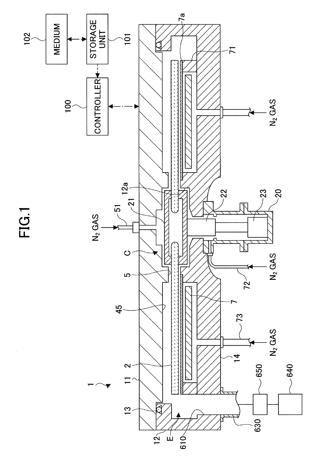
[0033][Film Deposition Apparatus]

[0034]An example of a film deposition apparatus according to a first embodiment of the present disclosure is described below with reference to FIGS. 1 through 5. The film deposition apparatus according to the first embodiment of the present disclosure is a film deposition apparatus to which the method for manufacturing the semiconductor device according to the first embodiment of the present disclosure is preferably applicable. Here, the film deposition apparatus is a so-called turntable type (described below) film deposition apparatus using a susceptor. Hence, the film deposition apparatus is described below by citing an example of the turntable type film deposition apparatus in which a film is deposited on surfaces of a plurality of substrates by supplying a process gas including a source gas to a predetermined supply region. Here, the susceptor for receiving the substrate is not necessarily formed as the turntable type, and a variety of film depos...

second embodiment

[0110]Next, a film deposition apparatus and a method for manufacturing a semiconductor device according to a second embodiment of the present disclosure are described below.

[0111][Film Deposition Apparatus]

[0112]FIG. 11 is a plan view illustrating an example of a film deposition apparatus according to a second embodiment. The film deposition apparatus according to the second embodiment and illustrated in FIG. 11 differs from the film deposition apparatus according to the first embodiment in that a process gas nozzle 34 is added to the second process region P2.

[0113]The process gas nozzle 34 is a gas supply unit to supply a reducing gas to a wafer W. A variety of gases may be used depending on the intended purpose as the reducing gas. For example, a hydrogen atom containing gas may be used as the reducing gas, and for example, hydrogen (H2), ammonia (NH3) and the like may be used as the reducing gas. When the second layer to be deposited in the film deposition process is an oxide fil...


PUM

PropertyMeasurementUnit
temperatureaaaaaaaaaa
diameteraaaaaaaaaa

Abstract

A method for manufacturing a semiconductor device is provided. In the method, impurities contained in a first layer formed on a substrate are removed by heating the first layer. On the first layer, a second layer is formed containing a component that forms a substance that is able to vaporize by reacting with the impurities.

Description

CROSS-REFERENCE TO RELATED APPLICATION[0001]The present application is based upon and claims priority to Japanese Patent Application No. 2017-232122, filed on Dec. 1, 2017, and Japanese Patent Application No. 2018-069515, filed on Mar. 30, 2018, the entire contents of which are incorporated herein by reference.BACKGROUND OF THE INVENTION1. Field of the Invention[0002]The present invention relates to a method for manufacturing a semiconductor device and a film deposition apparatus.2. Description of the Related Art[0003]In semiconductor devices, tungsten (W) is widely used as a material for filling a contact hole and the like formed in a semiconductor wafer (which is referred to as a “wafer” hereinafter) and its barrier material to prevent mutual diffusion, or used as a material for forming a gate electrode and the like of a transistor.[0004]The tungsten film is deposited by PVD (Physical Vapor Deposition) or CVD (Chemical Vapor Deposition), for example. In CVD, a method is known in w...

Claims


Application Information

Patent Timeline
Patent Type & Authority Applications(United States)
IPC IPC(8): H01L21/02H01L21/321H01L21/225H01L21/687H01L27/11582C23C16/40C23C16/06C23C16/455C23C16/52H10B43/27H10B43/35
CPCH01L21/02164H01L21/0228H01L21/68764C23C16/52H01L27/11582H01L21/02208H01L21/225C23C16/06C23C16/45544H01L21/68771H01L21/02299H01L21/321C23C16/401H01L21/02211H01L21/02271H01L21/02219C23C16/45551C23C16/45519C23C16/0281C23C16/14C23C16/402C23C16/56C23C16/0209H10B43/35H10B43/27H01L21/28556H01L21/324H01L21/67017H01L21/67098C23C16/44
Inventor UMEHARA, TAKAHITOKOAKUTSU, MASATO
Owner TOKYO ELECTRON LTD
Features
  • R&D
  • Intellectual Property
  • Life Sciences
  • Materials
  • Tech Scout
  • Unparalleled Data Quality
  • Higher Quality Content
  • 60% Fewer Hallucinations
Learn More