Nanosheet device with close source drain proximity

a technology of nanosheets and drains, applied in the field of electrical, electronic and computer arts, can solve the problem of high access resistance of devices, and achieve the effect of widening

Active Publication Date: 2019-06-20
IBM CORP
View PDF7 Cites 33 Cited by
  • Summary
  • Abstract
  • Description
  • Claims
  • Application Information

AI Technical Summary

Benefits of technology

[0008]A further method of fabricating nanosheet field-effect transistors includes obtaining a monolithic structure including a plurality of vertical stacks of monocrystalline silicon nanosheet channel layers and sacrificial silicon germanium layers, the nanosheet channel layers and sacrificial silicon germanium layers being arranged in alternating sequence and the sacrificial silicon germanium layers having greater widths than the widths of the nanosheet channel layers. Doped epitaxial extension regions are on the nanosheet channel layers. Inner spacers adjoin the silicon germanium layers and are vertically aligned with the doped epitaxial extension regions. The monolithic structure further includes epitaxial silicon germanium source / drain regions on the doped epitaxial extension regions, a plurality of dielectric dummy gates, each dielectric dummy gate extending vertically from a top surface of one of the vertical stacks, and a plurality of dielectric outer spacers, each of the outer spacers including a pair of vertical sidewalls adjoining one of the dielectric dummy gates. The dielectric dummy gates are removed to form trenches within the vertical sidewalls of the outer spacers. The sacrificial silicon germanium layers are removed selective to the nanosheet channel layers and the doped epitaxial extension regions to form spaces between the nanosheet channel layers without erosion of the source / drain regions. A gate dielectric layer is formed within the trenches and on the nanosheet channel layers and gate metal is deposited over the gate dielectric layer.

Problems solved by technology

The configurations of nanosheet devices as shown in FIG. 1F lead to difficulties in extension formation which can lead to higher access resistance in the devices.

Method used


Image

  • Nanosheet device with close source drain proximity
  • Nanosheet device with close source drain proximity
  • Nanosheet device with close source drain proximity

Examples


Embodiment Construction

[0025]Principles of the present invention will be described herein in the context of illustrative embodiments. It is to be appreciated, however, that the specific embodiments and / or methods illustratively shown and described herein are to be considered exemplary as opposed to limiting. Moreover, it will become apparent to those skilled in the art given the teachings herein that numerous modifications can be made to the embodiments shown that are within the scope of the claims. That is, no limitations with respect to the embodiments shown and described herein are intended or should be inferred.

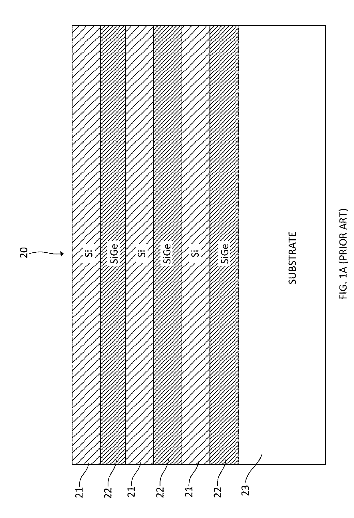
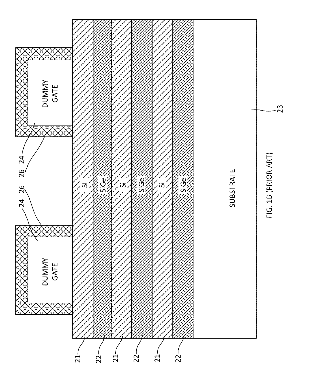
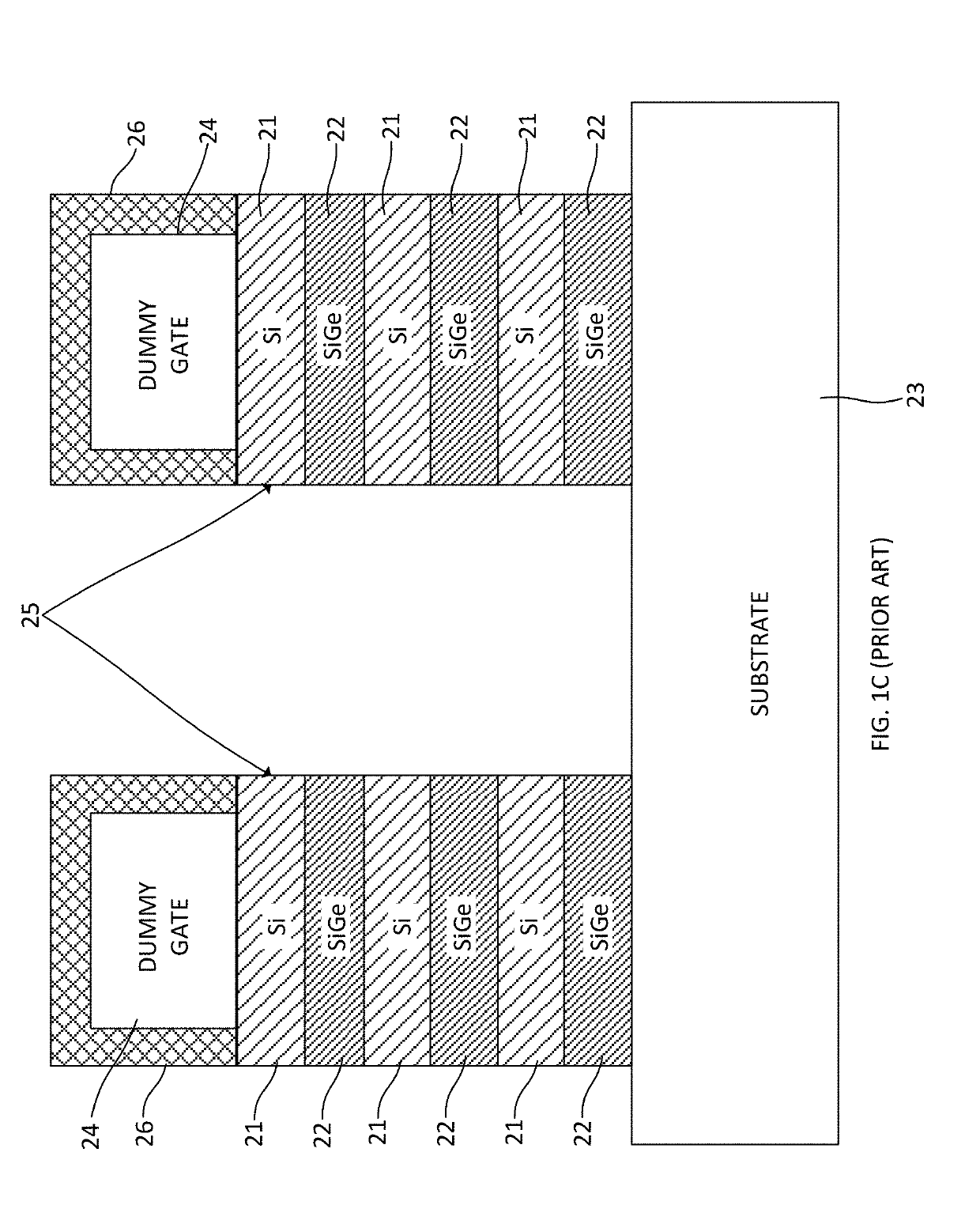
[0026]An exemplary sequence of steps that may be employed during fabrication of a nanosheet transistor including doped extensions is shown in FIGS. 2A-2G. The monolithic structure 40 shown in FIG. 2A is similar to that shown in FIG. 1C and can be obtained in the same manner described above. The same reference numerals are employed to designate the same or substantially similar elements. The str...


PUM


Abstract

A nanosheet transistor device having reduced access resistance is fabricated by recessing channel nanosheets and replacing the channel material with epitaxially grown doped extension regions. Sacrificial semiconductor layers between the channel nanosheets are selectively removed without damaging source/drain regions epitaxially grown on the extension regions. The sacrificial semiconductor layers are replaced by gate dielectric and gate metal layers.

Description

BACKGROUND[0001]The present invention relates generally to the electrical, electronic and computer arts and, more particularly, to nanosheet transistors and the formation of spacers in such transistors.[0002]With shrinking dimensions of various integrated circuit components, transistors such as field-effect transistors (FETs) have experienced dramatic improvements in both performance and power consumption. These improvements may be largely attributed to the reduction in dimensions of components used therein, which in general translate into reduced capacitance, resistance, and increased through-put current from the transistors. Metal oxide semiconductor field-effect transistors (MOSFETs) are well suited for use in high-density integrated circuits. As the size of MOSFETs and other devices decreases, the dimensions of source / drain regions, channel regions, and gate electrodes of the devices, also decrease.[0003]Nanosheet FETs have been under development for possible use in tight pitch ...

Claims


Application Information

Patent Timeline
Patent Type & Authority Applications(United States)
IPC IPC(8): H01L29/66H01L29/78H01L29/06H01L29/10H01L29/167H01L29/08
CPCH01L29/6681H01L29/7853H01L29/0653H01L29/1045H01L29/167H01L29/0673H01L29/66553H01L29/6653H01L29/0847H01L29/42392H01L21/30608H01L21/3065H01L29/78696H01L29/78618H01L29/66545H01L29/7848H01L29/165H01L29/775H01L29/66439H01L29/0843B82Y10/00H01L29/1079
Inventor BASKER, VEERARAGHAVAN S.MOCHIZUKI, SHOGOREZNICEK, ALEXANDER
Owner IBM CORP
Why Eureka
Try Eureka