Resin package and semiconductor light-emitting device

Active Publication Date: 2019-06-27
STANLEY ELECTRIC CO LTD
View PDF0 Cites 1 Cited by
  • Summary
  • Abstract
  • Description
  • Claims
  • Application Information

AI Technical Summary

Benefits of technology

[0021]According to the semiconductor light-emitting device using the resin package, the semiconductor light-emitting device can emit various colored lights having high reliability and a high light-emitting efficiency from the semiconductor light-emitting chip

Problems solved by technology

However, the above-described conventional semiconductor light-emitting device may include some challenges for manufacturing process, etc.
Furthermore, the blue light may degrade a quality of the epoxy resin, which forms the frame 32.
Therefore, the convent

Method used


Image

  • Resin package and semiconductor light-emitting device
  • Resin package and semiconductor light-emitting device
  • Resin package and semiconductor light-emitting device

Examples


Embodiment Construction

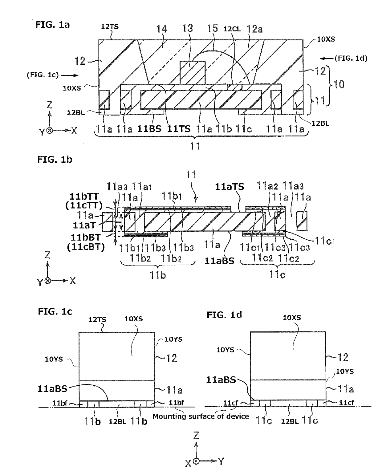
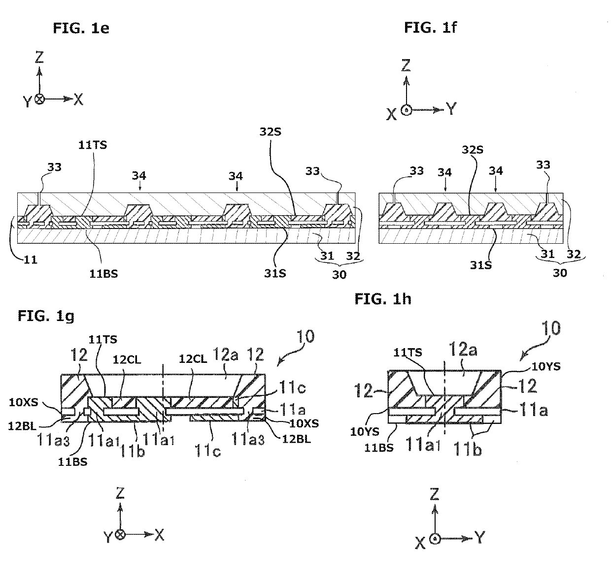
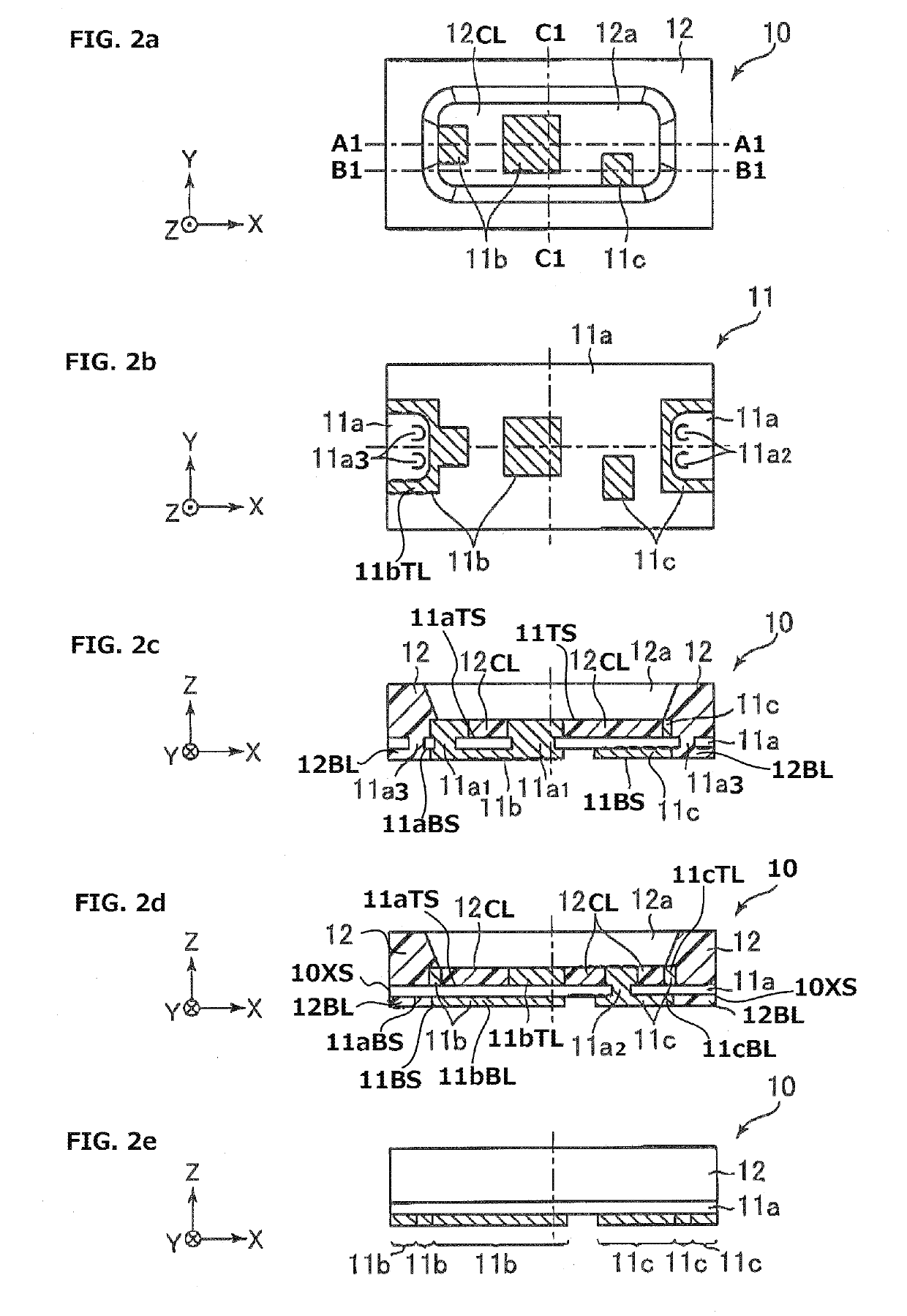
[0029]The present invention will now be described in detail with reference to FIG. 1a to FIG. 5g, in which the same, similar, or corresponding elements use the same reference marks. FIG. 1a is a schematic cross-sectional front view showing an exemplary embodiment of a semiconductor light-emitting device made in accordance with principles of the present invention.

[0030]The semiconductor light-emitting device of the exemplary embodiment can include: a resin package 10 having first side surfaces 10XS and second side surfaces 10YS located in a direction perpendicular to the first side surfaces 10XS including a printed circuit board 11 having a board top surface 11TS and a board bottom surface 11BS, a frame 12 and a cavity 12a, the frame 12 having a frame top surface 12TS including a frame cavity layer 12CL and a frame bottom layer 12 BL, and each of the first side surfaces 10XS located on opposite side of X-axis direction with respect to each other; a semiconductor light-emitting chip 1...


PUM


Abstract

Reliable resin packages and semiconductor light-emitting devices using the resin package can include a printed circuit board including a resin layer, metallic layers formed on a top surface of the resin layer and underneath a bottom surface of the resin layer and a frame arranged from a top surface of the printed circuit board toward a bottom surface of the printed circuit board. The semiconductor light-emitting device using the resin package can prevent the printed circuit board from warping toward the frame when forming the frame incorporating the printed circuit board because a total of each thickness of the metallic layers formed on the top surface and underneath the bottom surface of the resin layer can be thicker than a thickness of the resin layer. Thus, the present invention can provide the semiconductor light-emitting devices having high reliability, which can be used as a light source for vehicle lamps, etc.

Description

[0001]This application claims the priority benefit under 35 U.S.C. § 119 of Japanese Patent Application No. 2017-246310 filed on Dec. 22, 2017, which is hereby incorporated in its entirety by reference.BACKGROUND1. Field[0002]The present invention relates to resin packages and semiconductor light devices, and more particularly to the resin packages having a high quality and the semiconductor light-emitting devices using the resin package having the high quality such as a reliability, an assembly accuracy, and the like. Thus, the semiconductor light-emitting devices can be used as a reliable light source having a high light-efficiency for vehicle lamps, a general lighting, a back-lighting unit for a liquid crystal display, etc.2. Description of the Related Art[0003]Semiconductor light-emitting devices including a semiconductor light-emitting chip mounted in a resin package and manufacturing methods for the device are well known as disclosed in Patent Document No. 1 (Japanese Patent A...

Claims


Application Information

Patent Timeline
IPC IPC(8): H01L33/56H05K5/00H05K5/02H05K1/03
CPCH01L33/56H05K5/0091H05K5/02H05K1/0313H01L33/325H05K2201/0999H01L33/486H01L33/62H01L21/565H01L2924/181H01L2224/48227H01L2224/48091H01L2924/00012H01L2924/00014
Inventor WATANABE, SEISHIYOSHIMI, DAISUKETAI, KOHEI
Owner STANLEY ELECTRIC CO LTD
Why Eureka
Try Eureka